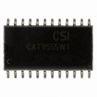
CAT9555WI-T1 ON Semiconductor, CAT9555WI-T1 Datasheet - Page 11

CAT9555WI-T1
Manufacturer Part Number
CAT9555WI-T1
Description
IC I/O EXPANDER I2C 16B 24SOIC
Manufacturer
ON Semiconductor
Datasheet
1.CAT9555WI-T1.pdf
(18 pages)
Specifications of CAT9555WI-T1
Interface
I²C, Serial, SMBus
Number Of I /o
16
Interrupt Output
Yes
Frequency - Clock
400kHz
Voltage - Supply
2.3 V ~ 5.5 V
Operating Temperature
-40°C ~ 85°C
Mounting Type
Surface Mount
Package / Case
24-SOIC (7.5mm Width)
Includes
POR
Lead Free Status / RoHS Status
Lead free / RoHS Compliant
Other names
9555WI-T2
CAT9555WI-T1TR
CAT9555WI-T2
CAT9555WI-T2TR
CAT9555WI-T2TR
CAT9555WI-T1TR
CAT9555WI-T2
CAT9555WI-T2TR
CAT9555WI-T2TR
Available stocks
Company
Part Number
Manufacturer
Quantity
Price
The output port register sets the outgoing logic levels
of the I/O ports, defined as outputs by the configu-
ration register. Bit values in this register have no effect
on I/O pins defined as inputs. Reads from the output
port register reflect the value that is in the flip-flop
controlling the output, not the actual I/O pin value.
The polarity inversion register allows the user to invert
the polarity of the input port register data. If a bit in
this register is set (“1”) the corresponding input port
data is inverted. If a bit in the polarity inversion
register is cleared (“0”), the original input port polarity
is retained.
The configuration register sets the directions of the
ports. Set the bit in the configuration register to enable
the corresponding port pin as an input with a high
impedance output driver. If a bit in this register is
cleared, the corresponding port pin is enabled as an
output. At power-up, the I/Os are configured as inputs
with a weak pull-up resistor to V
Writing to the Port Registers
Data is transmitted to the CAT9555 registers using the
write mode shown in Figure 8 and Figure 9.
FROM PORT 0
FROM PORT 1
© 2010 SCILLC. All rights reserved
Characteristics subject to change without notice
SDA
SCL
WRITE TO
DATA OUT
DATA OUT
start condition
PORT
S
SDA
SCL
1
0
start condition
S
2
1
1
0
3
0
slave address
2
1
4
0
3
0
slave address
A2 A1 A0
5
4
0
6
A2 A1 A0
5
7
6
R/W acknowledge
8
0
7
R/W acknowledge
9
A
from slave
8
0
CC
.
0
A
1
9
from slave
Figure 9. Write to Configuration Register
Figure 8. Write to Output Port Register
0
2
0
0
0
3
command byte
0
command byte
0
4
0
0
5
A
0
1
6
0
1
7
1
0
8
0
11
A
9
acknowledge
from slave
A
acknowledge
from slave
The CAT9555 registers are configured to operate at
four register pairs: Input Ports, Output Ports, Polarity
Inversion Ports and Configuration Ports. After sending
data to one register, the next data byte will be sent to
the other register in the pair. For example, if the first
byte of data is sent to the Configuration Port 1
(register 7), the next byte will be stored in the
Configuration Port 0 (register 6). Each 8-bit register
may be updated independently of the other registers.
Reading the Port Registers
The CAT9555 registers are read according to the
timing diagrams shown in Figure 10 and Figure 11.
Data from the register, defined by the command byte,
will be sent serially on the SDA line. Data is clocked
into the register on the failing edge of
acknowledge clock pulse. After the first byte is read,
additional data bytes may be read, but the second
read will reflect the data from the other register in the
pair. For example, if the first read is data from Input
Port 0, the next read data will be from Input Port 1.
The transfer is stopped when the master will not
acknowledge the data byte received and issue the
STOP condition.
MSB
0.7
1
2
data to configuration 0
3
data to port 0
DATA 0
DAT
4
A
5
0
6
7
0.0
t
pv
LSB
8
A
acknowledge
from slave
9
A
acknowledge
from slave
1.7
MSB
1
2
data to configuration 1
DATA 1
data to port 1
3
DATA 1
4
DATA VALID
Doc. No. MD-9003, Rev. J
5
t
1.0
pv
CAT9555
LSB A
A
P
stop
condition
the
P


