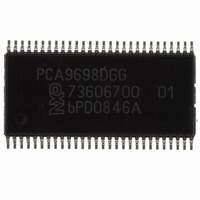
PCA9698DGG,512 NXP Semiconductors, PCA9698DGG,512 Datasheet - Page 16

PCA9698DGG,512
Manufacturer Part Number
PCA9698DGG,512
Description
IC I/O EXPANDER I2C 40B 56TSSOP
Manufacturer
NXP Semiconductors
Datasheet
1.PCA9698BS118.pdf
(48 pages)
Specifications of PCA9698DGG,512
Package / Case
56-TSSOP
Interface
I²C
Number Of I /o
40
Interrupt Output
Yes
Frequency - Clock
1MHz
Voltage - Supply
2.3 V ~ 5.5 V
Operating Temperature
-40°C ~ 85°C
Mounting Type
Surface Mount
Includes
POR
Logic Family
PCA9698
Number Of Lines (input / Output)
40.0 / 40.0
Operating Supply Voltage
2.3 V to 5.5 V
Power Dissipation
500 mW
Operating Temperature Range
- 40 C to + 85 C
Input Voltage
5.5 V
Logic Type
I2C Bus
Maximum Clock Frequency
1 MHz
Mounting Style
SMD/SMT
Number Of Input Lines
40.0
Number Of Output Lines
40.0
Output Current
50 mA
Output Voltage
5.5 V
Lead Free Status / RoHS Status
Lead free / RoHS Compliant
For Use With
OM6281 - DAUGHTER CARD PCA9698 FOR OM6275
Lead Free Status / Rohs Status
Lead free / RoHS Compliant
Other names
568-3241-5
935278614512
PCA9698DGG
935278614512
PCA9698DGG
Available stocks
Company
Part Number
Manufacturer
Quantity
Price
Part Number:
PCA9698DGG,512
Manufacturer:
NXP/恩智浦
Quantity:
20 000
NXP Semiconductors
PCA9698
Product data sheet
7.5 Device ID - PCA9698 ID field
The Device ID field is a 3 byte read-only (24 bits) word giving the following information:
The Device ID is read-only, hard-wired in the device and can be accessed as follows:
For the PCA9698, the Device ID is as shown in
1. START command
2. The master sends the Reserved Device ID I
3. The master sends the I
4. The master sends a Re-START command.
5. The master sends the Reserved Device ID I
6. The Device ID Read can be done, starting with the 12 manufacturer bits (first byte +
7. The master ends the reading sequence by NACKing the last byte, thus resetting the
Fig 10. PCA9698 ID field
•
•
•
12 bits with the manufacturer name, unique per manufacturer (e.g., NXP)
9 bits with the part identification, assigned by manufacturer (e.g., PCA9698)
3 bits with the die revision, assigned by manufacturer (e.g., RevX)
set to ‘0’ (write): ‘1111 1000’.
The LSB is a ‘Don’t care’ value. Only one device must acknowledge this byte (the one
that has the I
Remark: A STOP command followed by a START command will reset the slave state
machine and the Device ID Read cannot be performed. Also, a STOP command or a
Re-START command followed by an access to another slave device will reset the
slave state machine and the Device ID Read cannot be performed.
set to ‘1’ (read): ‘1111 1001’.
4 MSBs of the second byte), followed by the 9 part identification bits (4 LSBs of the
second byte + 5 MSBs of the third byte), and then the 3 die revision bits (3 LSBs of
the third byte).
slave device state machine and allowing the master to send the STOP command.
Remark: The reading of the Device ID can be stopped anytime by sending a NACK
command.
If the master continues to ACK the bytes after the third byte, the PCA9698 rolls back
to the first byte and keeps sending the Device ID sequence until a NACK has been
detected.
All information provided in this document is subject to legal disclaimers.
manufacturer
part identification
revision
2
C-bus slave address).
40-bit Fm+ I
Rev. 3 — 3 August 2010
2
0
C-bus slave address of the slave device it needs to identify.
0
2
0
C-bus advanced I/O port with RESET, OE and INT
0
0
0
0
0
0
Figure
2
2
C-bus address followed by the R/W bit
C-bus address followed by the R/W bit
0
0
10.
0
0
0
0
0
0
0
002aab942
0
0
0
PCA9698
0
0
0
© NXP B.V. 2010. All rights reserved.
16 of 48


