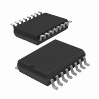
PCA9534D,118 NXP Semiconductors, PCA9534D,118 Datasheet - Page 4

PCA9534D,118
Manufacturer Part Number
PCA9534D,118
Description
IC I/O EXPANDER I2C 8B 16SOIC
Manufacturer
NXP Semiconductors
Datasheet
1.PCA9534BS118.pdf
(25 pages)
Specifications of PCA9534D,118
Package / Case
16-SOIC (0.300", 7.5mm Width)
Interface
I²C, SMBus
Number Of I /o
8
Interrupt Output
Yes
Frequency - Clock
400kHz
Voltage - Supply
2.3 V ~ 5.5 V
Operating Temperature
-40°C ~ 85°C
Mounting Type
Surface Mount
Includes
POR
Logic Family
PCA9534
Number Of Lines (input / Output)
8.0 / 8.0
Operating Supply Voltage
2.3 V to 5.5 V
Power Dissipation
200 mW
Operating Temperature Range
- 40 C to + 85 C
Input Voltage
5 V
Logic Type
I2C, SMBus
Maximum Clock Frequency
400 KHz
Mounting Style
SMD/SMT
Number Of Input Lines
8.0
Number Of Output Lines
8.0
Output Current
50 mA
Output Voltage
5 V
Operating Temperature (min)
-40C
Operating Temperature Classification
Industrial
Operating Temperature (max)
85C
Package Type
SO
Rad Hardened
No
Lead Free Status / RoHS Status
Lead free / RoHS Compliant
Lead Free Status / RoHS Status
Lead free / RoHS Compliant, Lead free / RoHS Compliant
Other names
568-1833-2
935275049118
PCA9534D-T
935275049118
PCA9534D-T
Available stocks
Company
Part Number
Manufacturer
Quantity
Price
Part Number:
PCA9534D,118
Manufacturer:
NXP/恩智浦
Quantity:
20 000
NXP Semiconductors
6. Functional description
PCA9534_3
Product data sheet
6.1.1 Command byte
6.1.2 Register 0 - Input Port register
6.1 Registers
Table 2.
[1]
Refer to
Table 3.
The command byte is the first byte to follow the address byte during a write transmission.
It is used as a pointer to determine which of the following registers will be written or read.
This register is a read-only port. It reflects the incoming logic levels of the pins, regardless
of whether the pin is defined as an input or an output by Register 3. Writes to this register
have no effect.
The default ‘X’ is determined by the externally applied logic level.
Symbol
IO6
IO7
INT
SCL
SDA
V
Command
0
1
2
3
DD
HVQFN package die supply ground is connected to both V
connected to supply ground for proper device operation. For enhanced thermal, electrical, and board level
performance, the exposed pad needs to be soldered to the board using a corresponding thermal pad on the
board and for proper heat conduction through the board, thermal vias need to be incorporated in the PCB in
the thermal pad region.
Figure 1 “Block diagram of
Pin description
Command byte
Pin
SO16, TSSOP16
11
12
13
14
15
16
Protocol
read byte
read/write byte
read/write byte
read/write byte
Rev. 03 — 6 November 2006
…continued
8-bit I
HVQFN16
9
10
11
12
13
14
Function
Input Port register
Output Port register
Polarity Inversion register
Configuration register
2
C-bus and SMBus low power I/O port with interrupt
PCA9534”.
Description
input/output 6
input/output 7
interrupt output (open-drain)
serial clock line
serial data line
supply voltage
SS
pin and exposed center pad. V
PCA9534
© NXP B.V. 2006. All rights reserved.
SS
pin must be
4 of 25


