HSP43220JC-25Z Intersil, HSP43220JC-25Z Datasheet - Page 18
HSP43220JC-25Z
Manufacturer Part Number
HSP43220JC-25Z
Description
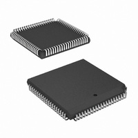
IC DECIMATING DGTL FILTER 84PLCC
Manufacturer
Intersil
Datasheet
1.HSP43220JC-25Z.pdf
(21 pages)
Specifications of HSP43220JC-25Z
Filter Type
Digital
Number Of Filters
4
Voltage - Supply
4.75 V ~ 5.25 V
Mounting Type
Surface Mount
Package / Case
84-PLCC
Lead Free Status / RoHS Status
Lead free / RoHS Compliant
Frequency - Cutoff Or Center
-
Max-order
-
Available stocks
Company
Part Number
Manufacturer
Quantity
Price


AC Electrical Specifications
NOTES:
Input Clock Frequency
FIR Clock Frequency
Input Clock Period
FIR Clock Period
Clock Pulse Width Low
Clock Pulse Width High
Clock Skew Between FIR_CK
and CK_IN
CK_IN Pulse Width Low
CK_IN Pulse Width High
CK_IN Setup to FIR_CK
CK_IN Hold from FIR_CK
RESET Pulse Width Low
Recovery Time on RESET
ASTARTIN Pulse Width Low
STARTOUT Delay from CK_IN
STARTIN Setup to CK_IN
Setup Time on DATA_IN
Hold Time on All inputs
Write Pulse Width Low
Write Pulse Width High
Setup Time on Address Bus Before the
Rising Edge of Write
Setup Time On-chip Select Before the
Rising Edge of Write
Setup Time on Control Bus Before the
Rising Edge of Write
DATA_RDY Pulse Width Low
DATA_OUT Delay Relative to FIR_CK
DATA RDY Valid Delay Relative
to FIR_CK
DATA_OUT Delay Relative to
OUT_SELH
Output Enable to Data Out Valid
Output Disable to Data Out
Three-State
Output Rise, Output Fall Times
5. Controlled by design or process parameters and not directly tested. Characterized upon initial design and after major process and/or design
6. Transition is measured at ±200mV from steady state voltage with loading as specified in test load circuit with and C
7. AC Testing is performed as follows: Input levels (CLK Input) 4.0V and 0V, Input levels (all other Inputs) 0V and 3.0V, Timing reference levels
8. Applies only when H_BYP = 1 or H_DRATE = 0.
changes.
(CLK) = 2.0V, (Others) = 1.5V, Output load per test load circuit and C
PARAMETER
18
V
tested at +25°C, unless otherwise specified. Temperature limits established by characterization and are
not production tested.
SYMBOL
CC
t
t
t
t
DRPWL
t
t
t
t
t
t
t
STADD
t
t
t
FIRDR
SPWH
RSPW
t
FIRDV
SPWL
CH1H
STOD
HOLD
t
t
F
CH1L
RTRS
t
t
STCS
STCB
t
F
t
t
t
STIC
t
t
OUT
OEV
OEZ
t
t
t
AST
SET
CIH
FIR
CIS
WH
WL
r
FIR
CK
SK
= +4.75V to +5.25V, T
CK
, t
f
(Notes 5, 8)
(Notes 5, 8)
(Notes 5, 8)
(Notes 5, 8)
(Note 6)
(Note 5)
from 0.8V to
2V, (Note 5)
NOTES
HSP43220
A
= 0°C to +70°C (Note 7). Parameters with MIN and/or MAX limits are 100%
2t
t
CK
L
FIR
4t
8t
MIN
= 40pF.
66
66
26
26
29
29
27
25
20
26
26
26
26
26
0
0
0
2
0
CK
CK
-
-
-
-
-
-
-
+ 10
- 20
-15
t
FIR
MAX
15
15
35
50
35
25
15
15
8
-
-
-
-
-
-
-
-
-
-
-
-
-
-
-
-
-
-
-
-
- 25
2t
t
CK
FIR
4t
8t
MIN
39
39
16
16
19
19
17
15
15
15
20
20
20
20
0
0
0
2
0
CK
CK
-
-
-
-
-
-
-
+ 10
- 10
-25
t
FIR
MAX
25.6
25.6
20
35
25
20
15
15
8
-
-
-
-
-
-
-
-
-
-
-
-
-
-
-
-
-
-
-
-
- 15
2t
t
CK
FIR
4t
8t
MIN
L
30
30
13
13
19
19
17
10
14
12
18
20
20
20
0
0
0
2
0
CK
CK
-
-
-
-
-
-
-
+ 10
= 40pF.
- 10
-33
t
FIR
MAX
33
33
18
28
20
20
15
15
6
-
-
-
-
-
-
-
-
-
-
-
-
-
-
-
-
-
-
-
-
- 15
October 10, 2008
FN2486.10
UNITS
MHz
MHz
ns
ns
ns
ns
ns
ns
ns
ns
ns
ns
ns
ns
ns
ns
ns
ns
ns
ns
ns
ns
ns
ns
ns
ns
ns
ns
ns
ns
Related parts for HSP43220JC-25Z
Image
Part Number
Description
Manufacturer
Datasheet
Request
R

Part Number:
Description:
Decimating Digital Filter
Manufacturer:
INTERSIL [Intersil Corporation]
Datasheet:

Part Number:
Description:
Decimating Digital Filter
Manufacturer:
Intersil Corporation
Datasheet:
Part Number:
Description:
Intersil Corporation [CMOS Serial Controller Interface]
Manufacturer:
Intersil Corporation
Datasheet:
Part Number:
Description:
Manufacturer:
Intersil Corporation
Datasheet:
Part Number:
Description:
357-036-542-201 CARDEDGE 36POS DL .156 BLK LOPRO
Manufacturer:
Intersil Corporation
Datasheet:
Part Number:
Description:
1024-Word x 4-Bit LSI Static RAM
Manufacturer:
Intersil Corporation
Datasheet:
Part Number:
Description:
General Purpose NPN Transistor Arrays FN341.4
Manufacturer:
Intersil Corporation
Datasheet:
Part Number:
Description:
CMOS 16-Bit Microprocessor
Manufacturer:
Intersil Corporation
Datasheet:
Part Number:
Description:
Manufacturer:
Intersil Corporation
Datasheet:
Part Number:
Description:
Manufacturer:
Intersil Corporation
Datasheet:
Part Number:
Description:
Manufacturer:
Intersil Corporation
Datasheet:
Part Number:
Description:
Manufacturer:
Intersil Corporation
Datasheet:
Part Number:
Description:
CMOS 6-Bit Latch and Decoder Memory Interfaces
Manufacturer:
Intersil Corporation
Datasheet:
Part Number:
Description:
CA3046General Purpose NPN Transistor Arrays
Manufacturer:
Intersil Corporation
Datasheet:
Part Number:
Description:
Manufacturer:
Intersil Corporation
Datasheet: