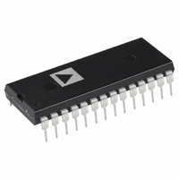
AD1893JN Analog Devices Inc, AD1893JN Datasheet - Page 6

AD1893JN
Manufacturer Part Number
AD1893JN
Description
IC SAMPLE-RATE CONV 16BIT 28DIP
Manufacturer
Analog Devices Inc
Series
SamplePort™r
Type
Sample Rate Converterr
Datasheet
1.AD1893JSTZRL.pdf
(20 pages)
Specifications of AD1893JN
Rohs Status
RoHS non-compliant
Applications
Multimedia
Voltage - Supply, Digital
2.7 V ~ 5.5 V
Mounting Type
Through Hole
Package / Case
28-DIP (0.600", 15.24mm)
Voltage - Supply, Analog
-
AD1893
Output Control Signals
Pin Name DIP LQFP I/O
BKPOL_O 19
MODE0_O 18
MODE1_O 17
Miscellaneous
Pin Name DIP
XTAL_O
XTAL_I
RESET
MUTE_O
MUTE_I
SETLSLW 28
PWRDWN 27
NC
Power Supply Connections
Pin Name
V
GND
DD
1
2
13
16
15
9, 20
DIP
7, 22
8, 14, 21
25
24
21
LQFP
40
42
14
20
18
38
36
1, 5, 8, 11,
12, 15, 17,
19, 22, 23,
26, 29, 33,
34, 37, 39,
41, 44
I
I
I
LQFP
6, 28
7, 16, 27
Description
Bit clock polarity. LO: Normal mode. Output data is valid on rising edges of BCLK_O, changed
on falling. HI: Inverted mode. Output data is valid on falling edges of BCLK_O, changed on
rising.
Serial mode zero control for output port.
Serial mode one control for output port.
MODE0_O
0
0
1
1
I/O
O
I
I
O
I
I
I
(F
with an external clock source.
memory pointer overlap. LO indicates normal operation.
MUTE_O. Reset LO for normal operation.
to sample clock jitter. LO: Fast-settling mode ( 200 ms). Some narrow-band noise
modulation may result from jitter on the LR clocks. This signal may be asynchronous with
respect to the crystal frequency, and dynamically changed, but is normally pulled up or
pulled down on a static basis.
operation.
Crystal output. Connect to one side of nominal 16 MHz crystal for sampling frequencies
Crystal input. Connect to other side of nominal 16 MHz crystal for sampling frequencies
Mute output. HI indicates that data is not currently valid due to read and write FIFO
Mute input. HI mutes the serial output to zeros (midscale). Normally connected to
Settle slowly to changes in sample rates. HI: Slow-settling mode ( 800 ms). Less sensitive
Power-down input. Set HI for inactive, low power dissipation state. Reset LO for normal
No connect. Reserved. Do not connect.
Description
(F
Active LO reset. Set HI for normal chip operation.
S
I/O
I
I
S
word rates) from 8 kHz to 56 kHz. Use this input to overdrive the on-chip oscillator
word rates) from 8 kHz to 56 kHz.
MODE1_O
0
1
0
1
Description
Positive digital voltage supply.
Digital ground. Pin 14 (DIP) and Pin 16 (LQFP) need not be decoupled.
Left-justified, no MSB delay, LR_O clock triggered.
Left-justified, MSB delay, LR_O clock triggered.
Right-justified, MSB delayed 16 bit clock periods from LR_O transition.
WCLK_O triggered, no MSB delay.
–6–
REV. A


