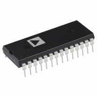
AD1893JN Analog Devices Inc, AD1893JN Datasheet - Page 10

AD1893JN
Manufacturer Part Number
AD1893JN
Description
IC SAMPLE-RATE CONV 16BIT 28DIP
Manufacturer
Analog Devices Inc
Series
SamplePort™r
Type
Sample Rate Converterr
Datasheet
1.AD1893JSTZRL.pdf
(20 pages)
Specifications of AD1893JN
Rohs Status
RoHS non-compliant
Applications
Multimedia
Voltage - Supply, Digital
2.7 V ~ 5.5 V
Mounting Type
Through Hole
Package / Case
28-DIP (0.600", 15.24mm)
Voltage - Supply, Analog
-
AD1893
A short delay corresponds to a large offset into the dense FIR
filter coefficient array, and a long delay corresponds to a small
offset. Note that because the output sample clock can arrive at
any arbitrary time with respect to the input sample clock, the
selection of a polyphase filter with which to convolve the input
sequence occurs on every output sample clock event. Occasion-
ally the FIFO which holds the input sequence in the FIR con-
volver is either not incremented, or incremented by two between
output sample clocks (see periods A and B in Figure 5); this
happens more often when the input and output sample clock
frequencies are dissimilar than when they are close together.
However, in this situation, an appropriate polyphase filter is
selected to process the input signal, and thus an accurate output
sample is computed. Input and output samples are not skipped
or repeated (unless the input FIFO underflows or overflows), as
is the case in some other sample rate converter implementations.
PAST
Figure 5. Input and Output Clock Event Relationship
SERVO CONTROL LOOP
SAMPLE CLOCK RATIO
(F
OFFSET INTO DENSE FIR FILTER COEFFICIENT ARRAY
LR_I
SIN
COMPUTE REQUESTED OUTPUT SAMPLE
)
TO ACCESS REQUIRED POLYPHASE FILTER
REQUIRED FILTER GROUP DELAY TO
OUTPUT SEQUENCE
(F
INPUT SEQUENCE
LR_O
A
SOUT
)
START
ADDRESS
DATA_I
B
BCLK_I
POLYPHASE FILTER
LR_I
ROM ADDRESS
COMPRESSION
SERIAL DATA
GENERATOR
GENERATOR
F
FREQUENCY
INPUT UNIT
SELECTOR
FIFO READ
RESPONSE
ADDRESS
SOUT
WCLK_I
Figure 6. Functional Block Diagram
FUTURE
< F
SIN
SMALL
OFFSET
LR_I
LR_O
LARGE
OFFSET
SHORT
DELAY
LONG
DELAY
AMPLITUDE
AMPLITUDE
COEFFICIENT
POLYPHASE
–10–
FIFO
ROM
GENERATOR
FIFO WRITE
ADDRESS
To obtain an accurate conversion, a large number of polyphase
filters are needed. The AD1893 SamplePort uses the equivalent
of 65,536 polyphase filters to achieve its high quality distortion
and dynamic range specifications.
Sample Clock Tracking
It should be clear that, in either model, the correct computation
of the ratio between the input sample rate (as determined from
the left/right input clock, LR_I) and the output sample rate (as
determined from the left/right output clock, LR_O) is critical to
the quality of the output data stream. It is straightforward to
compute this ratio if the sample rates are fixed and synchronous;
the challenge is to accurately track dynamically varying and
asynchronous sample rates, as well as to account for jitter.
The AD1893 SamplePort solves this problem by embedding the
ratio computation circuit within a digital servo control loop, as
shown in Figure 6. This control loop includes special provisions
to allow for the accurate tracking of dynamically changing
sample rates. The outputs of the control loop are the starting
read addresses for the input data FIFO and the filter coefficient
ROM. These start addresses are used by the FIFO and ROM
address generators, as shown in Figure 6.
The input data FIFO write address is generated by a counter
which is clocked by the input sample clock (i.e., LR_I). It is very
important that the FIFO read address and the FIFO write ad-
dress do not cross, as this means that the FIFO has either
underflowed or overflowed. This consideration affects the
choice of settling time of the control loop. When a step change
in the sample rate occurs, the relative positions of the read and
write addresses will change while the loop is settling. A fast
settling loop will act to keep the FIFO read and write addresses
separated better than a slow settling loop. The AD1893 includes
a user selectable pin (SETLSLW) to set the loop settling time
that essentially changes the coefficients of the digital servo con-
trol loop filter. The state of the SETLSLW pin can be changed
on-the-fly but is normally set and forgotten.
FIR CONVOLVER
LR_I
ACCUMULATOR
BCLK_O
SERIAL DATA
OUTPUT UNIT
WCLK_O
LR_O
DATA_O
REV. A


