STA013$ STMicroelectronics, STA013$ Datasheet - Page 15

STA013$
Manufacturer Part Number
STA013$
Description
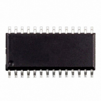
DECODER AUDIO MPEG 2.5 28-SOIC
Manufacturer
STMicroelectronics
Type
Audio Decoderr
Datasheet
1.STA013013TR.pdf
(38 pages)
Specifications of STA013$
Applications
Sound Cards, Players, Recorders
Voltage - Supply, Digital
2.4 V ~ 3.6 V
Mounting Type
Surface Mount
Package / Case
28-SOIC (7.5mm Width)
Audio Codec Type
MP3 Decoder
No. Of Dacs
1
No. Of Input Channels
2
No. Of Output Channels
2
Sampling Rate
48kSPS
Interface Type
I2C, Serial
Supply Voltage Range
2.4V To 3.6V
Rohs Compliant
Yes
Lead Free Status / RoHS Status
Lead free / RoHS Compliant
Voltage - Supply, Analog
-
Lead Free Status / Rohs Status
Compliant
Available stocks
Company
Part Number
Manufacturer
Quantity
Price
Part Number:
STA013$
Manufacturer:
ST
Quantity:
20 000
Company:
Part Number:
STA013$013TR
Manufacturer:
OV
Quantity:
4 500
MUTE
Address: 0x14
Type: R/W
Software Reset: 0x00
Hardware Reset: 0x00
X = don’t care; 0 = normal operation; 1 = mute
The MUTE command is handled according to the
state of the decoder, as described in section 2.5.
MUTE sets the clock running.
DATA_REQ_ENABLE
Address: 0x18
Type: R/W
Software Reset: 0x00
Hardware Reset: 0x00
The DATA_REQ_ENABLE register is used to
configure Pin n. 28 working as buffered output
clock or data request signal, used for multimedia
SYNCSTATUS
Address: 0x40
Type: RO
Software Reset: 0x00
Hardware Reset: 0x00
MSB
b7
X
MSB
MSB
b7
b7
X
X
X
b6
X
b6
b6
X
X
X
b5
X
b4
X
b5
b5
X
X
X
b3
X
b4
b4
X
X
X
b2
X
b1
b3
b3
X
X
X
X
LSB
b0
0
1
b2
b2
X
0
1
CMD_INTERRUPT
Address: 0x16
Type: R/W
Software Reset: 0x00
Hardware Reset: 0x00
X = don’t care;
0 = normal operation;
1 = write into I
The INTERRUPT is used to give STA013 the
command to write into the I2C/Ancillary Data
Buffer (Registers: 0x59 ... 0x5D). Every time the
Master has to extract the new buffer content (5
bytes) it writes into this register, setting it to a
non-zero value.
mode.
The buffered Output Clock has the same fre-
quency than the input clock (XTI)
MSB
b7
SS1
X
b1
b1
X
X
0
0
1
1
b6
X
LSB
LSB
SS0
b0
b0
X
X
0
1
0
1
STA013 - STA013B - STA013T
2
b5
X
C/Ancillary Data
b4
X
Research of sync word
Wait for Confirmation
buffered output clock
b3
X
request signal
Synchronised
Description
Description
not used
b2
X
b1
X
LSB
15/38
b0
0
1


