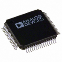
ADV7343BSTZ Analog Devices Inc, ADV7343BSTZ Datasheet - Page 46

ADV7343BSTZ
Manufacturer Part Number
ADV7343BSTZ
Description
IC ENCODER VIDEO W/DAC 64-LQFP
Manufacturer
Analog Devices Inc
Type
Video Encoderr
Datasheet
1.ADV7343BSTZ.pdf
(104 pages)
Specifications of ADV7343BSTZ
Applications
DVD, Blu-Ray
Voltage - Supply, Analog
3.3V
Voltage - Supply, Digital
1.8V
Mounting Type
Surface Mount
Package / Case
64-LQFP
Supply Voltage Range
1.71V To 1.89V
Operating Temperature Range
-40°C To +85°C
Tv / Video Case Style
LQFP
No. Of Pins
64
Svhc
No SVHC (18-Jun-2010)
Operating Temperature Max
85°C
Operating
RoHS Compliant
Input Format
Digital
Output Format
Analogue
Dac Resolution
11bit
Rohs Compliant
Yes
Lead Free Status / RoHS Status
Lead free / RoHS Compliant
Available stocks
Company
Part Number
Manufacturer
Quantity
Price
Company:
Part Number:
ADV7343BSTZ
Manufacturer:
ADI
Quantity:
301
Company:
Part Number:
ADV7343BSTZ
Manufacturer:
Analog Devices Inc
Quantity:
10 000
Part Number:
ADV7343BSTZ
Manufacturer:
ADI/亚德诺
Quantity:
20 000
Company:
Part Number:
ADV7343BSTZ-3
Manufacturer:
ADI
Quantity:
246
ADV7342/ADV7343
INPUT CONFIGURATION
The ADV7342/ADV7343 support a number of different input
modes. The desired input mode is selected using Subaddress
0x01, Bits[6:4]. The ADV7342/ADV7343 default to standard
definition only (SD only) on power-up. Table 36 provides an
overview of all possible input configurations. Each input mode
is described in detail in the following sections.
STANDARD DEFINITION ONLY
Subaddress 0x01, Bits[6:4] = 000
Standard definition (SD) YCrCb data can be input in 4:2:2 format.
Standard definition (SD) RGB data can be input in 4:4:4 format.
A 27 MHz clock signal must be provided on the CLKIN_A pin.
Input synchronization signals are provided on the S_HSYNC
and S_VSYNC pins.
8-Bit 4:2:2 YCrCb Mode
Subaddress 0x87, Bit 7 = 0; Subaddress 0x88, Bit 3 = 0
In 8-bit 4:2:2 YCrCb input mode, the interleaved pixel data is
input on Pin S7 to Pin S0 (or Pin Y7 to Pin Y0, depending on
Subaddress 0x01, Bit 7), with Pin S0/Y0 being the LSB. The
Table 36. Input Configuration
Input Mode
000
001
010
011
100
111
1
2
3
4
5
The input mode is determined by Subaddress 0x01, Bits[6:4].
In SD only (YCrCb) mode, the format of the input data is determined by Subaddress 0x88, Bits[4:3]. See Table 29 for more information.
External synchronization signals must be used in this input mode. Embedded EAV/SAV timing codes are not supported.
In ED/HD-SDR only (YCrCb) mode, the format of the input data is determined by Subaddress 0x33, Bit 6. See Table 22 for more information.
ED = enhanced definition = 525p and 625p.
SD only
8-bit YCrCb
16-bit YCrCb
8-bit YCrCb
16-bit YCrCb
24-bit RGB
ED/HD-SDR only
16-bit YCrCb
24-bit YCrCb
24-bit RGB
ED/HD-DDR only (8-bit)
SD and ED/HD-SDR (24-bit)
SD and ED/HD-DDR (16-bit)
ED only (54 MHz) (8-bit)
1
3
3
2
2
2, 3
2, 3
4, 5
5
5
5
5
7
6
5
YCrCb (SD)
YCrCb (SD)
YCrCb
4
Cr
S
Y
R
R
3
2
Rev. A | Page 46 of 104
ED/HD RGB input enable (Subaddress 0x35[1]) = 0
ED/HD RGB input enable (Subaddress 0x35[1]) = 1
1
SD RGB input enable (Subaddress 0x87[7]) = 1
Y/C/S bus swap (Subaddress 0x01[7]) = 0
Y/C/S bus swap (Subaddress 0x01[7]) = 1
0
7
ITU-R BT.601/656 input standard is supported. Embedded
EAV/SAV timing codes are also supported.
16-Bit 4:2:2 YCrCb Mode
Subaddress 0x87, Bit 7 = 0; Subaddress 0x88, Bit 3 = 1
In 16-bit 4:2:2 YCrCb input mode, the Y pixel data is input on
Pin S7 to Pin S0 (or Pin Y7 to Pin Y0, depending on Subaddress
0x01, Bit 7), with Pin S0/Y0 being the LSB.
The CrCb pixel data is input on Pin Y7 to Pin Y0 (or Pin C7 to
Pin C0, depending on Subaddress 0x01, Bit 7), with Pin Y0/C0
being the LSB. Embedded EAV/SAV timing codes are not
supported, so an external synchronization is needed in this mode.
24-Bit 4:4:4 RGB Mode
Subaddress 0x87, Bit 7 = 1
In 24-bit 4:4:4 RGB input mode, the red pixel data is input on
Pin S7 to Pin S0, the green pixel data is input on Pin Y7 to
Pin Y0, and the blue pixel data is input on Pin C7 to Pin C0.
The S0, Y0, and C0 pinsare the respective bus LSBs.
6
YCrCb (ED/HD)
5
Y (ED/HD)
YCrCb
YCrCb
YCrCb
4
CrCb
Y
G
G
Y
Y
Y
3
2
1
0
7
6
5
CrCb (ED/HD)
4
CrCb
CrCb
Cb
C
B
B
3
2
1
0


