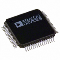
ADV7343BSTZ Analog Devices Inc, ADV7343BSTZ Datasheet - Page 20

ADV7343BSTZ
Manufacturer Part Number
ADV7343BSTZ
Description
IC ENCODER VIDEO W/DAC 64-LQFP
Manufacturer
Analog Devices Inc
Type
Video Encoderr
Datasheet
1.ADV7343BSTZ.pdf
(104 pages)
Specifications of ADV7343BSTZ
Applications
DVD, Blu-Ray
Voltage - Supply, Analog
3.3V
Voltage - Supply, Digital
1.8V
Mounting Type
Surface Mount
Package / Case
64-LQFP
Supply Voltage Range
1.71V To 1.89V
Operating Temperature Range
-40°C To +85°C
Tv / Video Case Style
LQFP
No. Of Pins
64
Svhc
No SVHC (18-Jun-2010)
Operating Temperature Max
85°C
Operating
RoHS Compliant
Input Format
Digital
Output Format
Analogue
Dac Resolution
11bit
Rohs Compliant
Yes
Lead Free Status / RoHS Status
Lead free / RoHS Compliant
Available stocks
Company
Part Number
Manufacturer
Quantity
Price
Company:
Part Number:
ADV7343BSTZ
Manufacturer:
ADI
Quantity:
301
Company:
Part Number:
ADV7343BSTZ
Manufacturer:
Analog Devices Inc
Quantity:
10 000
Part Number:
ADV7343BSTZ
Manufacturer:
ADI/亚德诺
Quantity:
20 000
Company:
Part Number:
ADV7343BSTZ-3
Manufacturer:
ADI
Quantity:
246
ADV7342/ADV7343
PIN CONFIGURATION AND FUNCTION DESCRIPTIONS
Table 15. Pin Function Descriptions
Pin No.
13, 12,
9 to 4
29 to 25,
18 to 16
62 to 58,
55 to 53
52, 51, 15,
14, 3, 2
30
63
50
49
22
23
24
48
47
Mnemonic
Y7 to Y0
C7 to C0
S7 to S0
TEST5 to
TEST0
CLKIN_A
CLKIN_B
S_HSYNC
S_VSYNC
P_HSYNC
P_VSYNC
P_BLANK
SFL
R
SET1
Input/
Output
I
I
I
I
I
I
I/O
I/O
I
I
I
I/O
I
V
TEST0
TEST1
TEST2
TEST3
DGND
DD_IO
V
Y0
Y1
Y2
Y3
Y4
Y5
Y6
Y7
C0
DD
10
11
12
13
14
15
16
1
3
9
2
4
5
6
7
8
Description
8-Bit Pixel Port. Y0 is the LSB. Refer to Table 36 for input modes.
8-Bit Pixel Port. C0 is the LSB. Refer to Table 36 for input modes.
8-Bit Pixel Port. S0 is the LSB. Refer to Table 36 for input modes.
Unused. These pins should be connected to DGND.
Pixel Clock Input for HD Only (74.25 MHz), ED
Pixel Clock Input for Dual Modes Only. Requires a 27 MHz reference clock for ED operation or a
74.25 MHz reference clock for HD operation.
SD Horizontal Synchronization Signal. This pin can also be configured to output an SD, ED, or HD
horizontal synchronization signal. See the External Horizontal and Vertical Synchronization
Control section.
SD Vertical Synchronization Signal. This pin can also be configured to output an SD, ED, or HD
vertical synchronization signal. See the External Horizontal and Vertical Synchronization Control
section.
ED/HD Horizontal Synchronization Signal. See the External Horizontal and Vertical
Synchronization Control section.
ED/HD Vertical Synchronization Signal. See the External Horizontal and Vertical Synchronization
Control section.
ED/HD Blanking Signal. See the External Horizontal and Vertical Synchronization Control section.
Subcarrier Frequency Lock (SFL) Input. The SFL input is used to drive the color subcarrier DDS
system, timing reset, or subcarrier reset.
This pin is used to control the amplitudes of the DAC 1, DAC 2, and DAC 3 outputs. For full-drive
operation (for example, into a 37.5 Ω load), a 510 Ω resistor must be connected from R
AGND. For low-drive operation (for example, into a 300 Ω load), a 4.12 kΩ resistor must be
connected from R
64
17 18 19 20 21 22 23 24 25 26 27 28 29 30 31 32
63 62 61 60 59 58 57 56 55 54 53 52 51 50 49
PIN 1
ADV7342/ADV7343
Figure 20. Pin Configuration
Rev. A | Page 20 of 104
SET1
(Not to Scale)
TOP VIEW
to AGND.
1
Only (27 MHz or 54 MHz), or SD Only (27 MHz).
48
46
40
47
45
44
43
42
41
39
38
37
36
35
34
33
SFL
R
V
COMP1
DAC 1
DAC 2
DAC 3
V
AGND
DAC 4
DAC 5
DAC 6
R
COMP2
PV
EXT_LF1
SET1
REF
AA
SET2
DD
SET1
to


