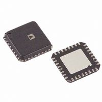
ADV7391BCPZ Analog Devices Inc, ADV7391BCPZ Datasheet - Page 40

ADV7391BCPZ
Manufacturer Part Number
ADV7391BCPZ
Description
IC ENCODER VIDEO W/DAC 32-LFCSP
Manufacturer
Analog Devices Inc
Type
Video Encoderr
Datasheet
1.ADV7393BCPZ.pdf
(108 pages)
Specifications of ADV7391BCPZ
Applications
Set-Top Boxes, Video Players, Displays
Voltage - Supply, Analog
2.6 V ~ 3.46 V
Voltage - Supply, Digital
1.71 V ~ 1.89 V
Mounting Type
Surface Mount
Package / Case
32-LFCSP
Supply Voltage Range
1.71V To 1.89V
Operating Temperature Range
-40°C To +85°C
Tv / Video Case Style
LFCSP
No. Of Pins
32
Svhc
No SVHC (18-Jun-2010)
Operating Temperature Max
85°C
Operating
RoHS Compliant
Input Format
Digital
Output Format
Analogue
Dac Resolution
10bit
Rohs Compliant
Yes
Lead Free Status / RoHS Status
Lead free / RoHS Compliant
For Use With
EVAL-ADV7391EBZ - BOARD EVAL FOR ADV7391 ENCODER
Lead Free Status / RoHS Status
Lead free / RoHS Compliant
Available stocks
Company
Part Number
Manufacturer
Quantity
Price
Company:
Part Number:
ADV7391BCPZ
Manufacturer:
CIRRUS
Quantity:
7 400
Company:
Part Number:
ADV7391BCPZ
Manufacturer:
ADI
Quantity:
302
Part Number:
ADV7391BCPZ
Manufacturer:
ADI/亚德诺
Quantity:
20 000
Company:
Part Number:
ADV7391BCPZ-3
Manufacturer:
AD
Quantity:
1 831
Company:
Part Number:
ADV7391BCPZ-REEL
Manufacturer:
HIT
Quantity:
530
Part Number:
ADV7391BCPZ-REEL
Manufacturer:
ADI/亚德诺
Quantity:
20 000
ADV7390/ADV7391/ADV7392/ADV7393
SR7 to
SR0
0x8B
0x8C
0x8D
0x8E
0x8F
0x90
0x91
0x92
0x93
0x94
0x95
0x96
0x97
0x98
1
2
3
x = Logic 0 or Logic 1.
X = don’t care.
SD subcarrier frequency registers default to NTSC subcarrier frequency values.
Register
SD Timing Register 1
Note: Applicable in
master modes only,
that is, Subaddress
0x8A, Bit 0 = 1.
SD F
SD F
SD F
SD F
SD F
SD Closed Captioning
SD Closed Captioning
SD Closed Captioning
SD Closed Captioning
SD Pedestal Register 0
SD Pedestal Register 1
SD Pedestal Register 2
SD Pedestal Register 3
SC
SC
SC
SC
SC
Register 0
Register 1
Register 2
Register 3
Phase
3
3
3
3
Bit Description
SD HSYNC width
SD HSYNC to VSYNC delay
SD HSYNC to VSYNC rising
edge delay (Mode 1 only)
SD VSYNC Wwth (Mode 2 only)
SD HSYNC to pixel data adjust
Subcarrier Frequency Bits[7:0]
Subcarrier Frequency Bits[15:8]
Subcarrier Frequency Bits[23:16]
Subcarrier Frequency Bits[31:24]
Subcarrier Phase Bits[9:2]
Extended data on even fields
Extended data on even fields
Data on odd fields
Data on odd fields
Pedestal on odd fields
Pedestal on odd fields
Pedestal on even fields
Pedestal on even fields
Rev. B | Page 40 of 108
x
7
0
0
1
1
x
x
x
x
x
x
x
x
17
25
17
25
6
0
1
0
1
x
x
x
x
x
16
x
x
x
x
24
16
24
5
X
X
0
0
1
1
x
x
x
x
x
x
15
x
x
x
23
15
23
2
2
Bit Number
4
0
1
0
1
0
1
x
x
x
x
x
x
x
x
x
14
22
14
22
3
0
0
1
1
x
x
x
x
x
x
x
x
x
13
21
13
21
1
2
0
1
0
1
x
x
x
x
x
x
x
x
x
12
20
12
20
1
0
0
1
1
x
x
x
x
x
x
x
x
x
11
19
11
19
0
0
1
0
1
x
x
x
x
x
x
x
x
x
10
18
10
18
Register Setting
t
t
t
t
t
t
t
t
t
t
One clock cycle.
Four clock cycles.
16 clock cycles.
128 clock cycles.
0 clock cycles.
One clock cycle.
Two clock cycles.
Three clock cycles.
Subcarrier Frequency
Bits[7:0].
Subcarrier Frequency
Bits[15:8].
Subcarrier Frequency
Bits[23:16].
Subcarrier Frequency
Bits[31:24].
Subcarrier Phase Bits[9:2].
Extended Data Bits[7:0].
Extended Data Bits[15:8].
Data Bits[7:0].
Data Bits[15:8].
Setting any of these bits
to 1 disables the
pedestal on the line
number indicated by
the bit settings.
a
a
a
a
b
b
b
b
c
c
= one clock cycle.
= four clock cycles.
= 16 clock cycles.
= 128 clock cycles.
= t
= t
= 0 clock cycles.
= four clock cycles.
= eight clock cycles.
= 18 clock cycles.
b.
b
+ 32 μs.
Reset
Value
0x00
0x1F
0x7C
0xF0
0x21
0x00
0x00
0x00
0x00
0x00
0x00
0x00
0x00
0x00


