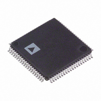
ADV7194KSTZ Analog Devices Inc, ADV7194KSTZ Datasheet - Page 45

ADV7194KSTZ
Manufacturer Part Number
ADV7194KSTZ
Description
IC ENCODER VIDEO EXT-10 80-LQFP
Manufacturer
Analog Devices Inc
Type
Video Encoderr
Datasheet
1.ADV7194KSTZ.pdf
(69 pages)
Specifications of ADV7194KSTZ
Applications
DVD, PC Video, Multimedia
Voltage - Supply, Analog
3.3 V ~ 5 V
Voltage - Supply, Digital
3.3 V ~ 5 V
Mounting Type
Surface Mount
Package / Case
80-LQFP
Input Format
Digital
Output Format
Analog
Supply Voltage Range
3.15V To 3.6V
Operating Temperature Range
0°C To +70°C
Tv / Video Case Style
LQFP
No. Of Pins
80
Msl
MSL 1 - Unlimited
Svhc
No SVHC
Rohs Compliant
Yes
Lead Free Status / RoHS Status
Lead free / RoHS Compliant
For Use With
EVAL-ADV7194EB - BOARD EVAL FOR ADV7194
Lead Free Status / RoHS Status
Lead free / RoHS Compliant, Lead free / RoHS Compliant
Available stocks
Company
Part Number
Manufacturer
Quantity
Price
Company:
Part Number:
ADV7194KSTZ
Manufacturer:
ADI
Quantity:
393
Company:
Part Number:
ADV7194KSTZ
Manufacturer:
ADI
Quantity:
717
Company:
Part Number:
ADV7194KSTZ
Manufacturer:
Analog Devices Inc
Quantity:
10 000
Part Number:
ADV7194KSTZ
Manufacturer:
ADI/亚德诺
Quantity:
20 000
The ADV7194 is a highly integrated circuit containing both
precision analog and high-speed digital circuitry. It has been
designed to minimize interference effects on the integrity of the
analog circuitry by the high-speed digital circuitry. It is impera-
tive that these same design and layout techniques be applied
to the system level design such that high-speed, accurate perfor-
mance is achieved. The Recommended Analog Circuit Layout
shows the analog interface between the device and monitor.
The layout should be optimized for lowest noise on the ADV7194
power and ground lines by shielding the digital inputs and pro-
viding good decoupling. The lead length between groups of
V
to minimize inductive ringing.
Ground Planes
The ground plane should encompass all ADV7194 ground pins,
voltage reference circuitry, power supply bypass circuitry for
the ADV7194, the analog output traces, and all the digital signal
traces leading up to the ADV7194. This should be as substantial
as possible to maximize heat spreading and power dissipation on
the board.
Power Planes
The ADV7194 and any associated analog circuitry should have
its own power plane, referred to as the analog power plane (V
This power plane should be connected to the regular PCB power
plane (V
should be located within three inches of the ADV7194.
The metallization gap separating device power plane and board
power plane should be as narrow as possible to minimize the
obstruction to the flow of heat from the device into the gen-
eral board.
The PCB power plane should provide power to all digital logic
on the PC board, and the analog power plane should provide
power to all ADV7194 power pins and voltage reference circuitry.
Plane-to-plane noise coupling can be reduced by ensuring that
portions of the regular PCB power and ground planes do not
overlay portions of the analog power plane, unless they can be
arranged such that the plane-to-plane noise is common-mode.
AA
, AGND, V
CC
) at a single point through a ferrite bead. This bead
DD
, and DGND pins should be minimized so as
BOARD DESIGN AND LAYOUT CONSIDERATIONS
APPENDIX 1
AA
).
Supply Decoupling
For optimum performance, bypass capacitors should be installed
using the shortest leads possible, consistent with reliable operation,
to reduce the lead inductance. Best performance is obtained
with 0.1 µF ceramic capacitor decoupling. Each group of V
pins on the ADV7194 must have at least one 0.1 µF decoupling
capacitor to AGND. The same applies to groups of V
DGND. These capacitors should be placed as close as possible
to the device.
It is important to note that while the ADV7194 contains cir-
cuitry to reject power supply noise, this rejection decreases with
frequency. If a high frequency switching power supply is used,
the designer should pay close attention to reducing power sup-
ply noise and consider using a three-terminal voltage regulator
for supplying power to the analog power plane.
Digital Signal Interconnect
The digital inputs to the ADV7194 should be isolated as much
as possible from the analog outputs and other analog cir-
cuitry. Also, these input signals should not overlay the analog
power plane.
Due to the high clock rates involved, long clock lines to the
ADV7194 should be avoided to reduce noise pickup.
Any active termination resistors for the digital inputs should be
connected to the regular PCB power plane (V
analog power plane.
Analog Signal Interconnect
The ADV7194 should be located as close as possible to the out-
put connectors to minimize noise pickup and reflections due to
impedance mismatch.
The video output signals should overlay the ground plane, and
not the analog power plane, to maximize the high frequency power
supply rejection.
Digital inputs, especially pixel data inputs and clocking signals
should never overlay any of the analog signal circuitry and should
be kept as far away as possible.
For best performance, the outputs should each have a 300 Ω load
resistor connected to AGND. These resistors should be placed
as close as possible to the ADV7194 so as to minimize reflections.
The ADV7194 should have no inputs left floating. Any inputs
that are not required should be tied to ground.
ADV7194
CC
), and not the
DD
and
AA


