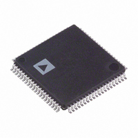
ADV7194KSTZ Analog Devices Inc, ADV7194KSTZ Datasheet - Page 33

ADV7194KSTZ
Manufacturer Part Number
ADV7194KSTZ
Description
IC ENCODER VIDEO EXT-10 80-LQFP
Manufacturer
Analog Devices Inc
Type
Video Encoderr
Datasheet
1.ADV7194KSTZ.pdf
(69 pages)
Specifications of ADV7194KSTZ
Applications
DVD, PC Video, Multimedia
Voltage - Supply, Analog
3.3 V ~ 5 V
Voltage - Supply, Digital
3.3 V ~ 5 V
Mounting Type
Surface Mount
Package / Case
80-LQFP
Input Format
Digital
Output Format
Analog
Supply Voltage Range
3.15V To 3.6V
Operating Temperature Range
0°C To +70°C
Tv / Video Case Style
LQFP
No. Of Pins
80
Msl
MSL 1 - Unlimited
Svhc
No SVHC
Rohs Compliant
Yes
Lead Free Status / RoHS Status
Lead free / RoHS Compliant
For Use With
EVAL-ADV7194EB - BOARD EVAL FOR ADV7194
Lead Free Status / RoHS Status
Lead free / RoHS Compliant, Lead free / RoHS Compliant
Available stocks
Company
Part Number
Manufacturer
Quantity
Price
Company:
Part Number:
ADV7194KSTZ
Manufacturer:
ADI
Quantity:
393
Company:
Part Number:
ADV7194KSTZ
Manufacturer:
ADI
Quantity:
717
Company:
Part Number:
ADV7194KSTZ
Manufacturer:
Analog Devices Inc
Quantity:
10 000
Part Number:
ADV7194KSTZ
Manufacturer:
ADI/亚德诺
Quantity:
20 000
MODE REGISTER 5
MR5 (MR57–MR50)
(Address (SR4–SR0) = 05H)
Mode Register 5 is an 8-bit-wide register. Figure 60 shows
the various operations under the control of Mode Register 5.
MR5 BIT DESCRIPTION
Y-Level Control (MR50)
This bit controls the component Y output level on the ADV7194.
If this bit is set (0), the encoder outputs Betacam levels when
configured in PAL or NTSC mode. If this bit is set (1), the
encoder outputs SMPTE levels when configured in PAL or
NTSC mode.
UV-Level Control (MR51–MR52)
These bits control the component U and V output levels on
the ADV7194. It is possible to have UV levels with a peak-to-
peak amplitude of either 700 mV (MR52 + MR51 = 01) or
1000 mV (MR52 + MR51 = 10) in NTSC and PAL. It is also
possible to have default values of 934 mV for NTSC and 700 mV
for PAL (MR52 + MR51 = 00).
MR47
0
1
MODE CONTROL
MR57
INTERLACED
INTERLACED
NONINTERLACED
0
1
POSITION
FRONT PORCH
BACK PORCH
CLAMP
MR57
MR47
MR46
0
1
MR56
COLOR BAR
CONTROL
CLAMP DELAY
0
1
DISABLE
ENABLE
MR56
DIRECTION
MR46
POSITIVE
NEGATIVE
MR45
0
1
MR55 MR54
CONTROL
ENABLE BURST
DISABLE BURST
0
0
1
1
BURST
MR55
MR45
CLAMP DELAY
0
1
0
1
MR44
0
1
CHROMINANCE
NO DELAY
1
2
3
ENABLE COLOR
DISABLE COLOR
CONTROL
MR54
PCLK
PCLK
PCLK
MR44
MR43
MR53
0
1
0
1
RGB SYNC
720 PIXELS
710 PIXELS/702 PIXELS
RGB Sync (MR53)
This bit is used to set up the RGB outputs with the sync infor-
mation encoded on all RGB outputs.
Clamp Delay (MR54–MR55)
These bits control the delay or advance of the CLAMP signal in
the front or back porch of the ADV7194. It is possible to delay or
advance the pulse by zero, one, two, or three clock cycles.
Note: TTX functionality is shared with VSO and CLAMP on Pin
62. CLAMP/VSO Select (MR77) and TTX Input/CLAMP/VSO
Output (MR76) have to be set accordingly.
Clamp Delay Direction (MR56)
This bit controls a positive or negative delay in the CLAMP sig-
nal. If this bit is set (1), the delay is negative. If it is set (0), the
delay is positive.
Clamp Position (MR57)
This bit controls the position of the CLAMP signal. If this bit is
set (1), the CLAMP signal is located in the back porch position.
If this bit is set (0), the CLAMP signal is located in the front
porch position.
LINE DURATION
MR53
ACTIVE VIDEO
DISABLE
ENABLE
MR43
MR52 MR51
MR42 MR41
0
0
1
1
0
0
1
1
UV-LEVEL CONTROL
MR52
MR42
0
1
0
1
GENLOCK CONTROL
0
1
0
1
DEFAULT LEVELS
700mV
1000mV
RESERVED
DISABLE GENLOCK
ENABLE SUBCARRIER
RESET PIN
TIMING RESET
ENABLE RTC PIN
MR51
MR41
MR50
0
1
MR40
CONTROL
Y-LEVEL
0
1
DISABLE
ENABLE
MR50
VSYNC 3H
MR40
CONTROL
DISABLE
ENABLE
ADV7194


