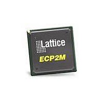
LFE2-12SE-5TN144C Lattice, LFE2-12SE-5TN144C Datasheet - Page 42

LFE2-12SE-5TN144C
Manufacturer Part Number
LFE2-12SE-5TN144C
Description
FPGA - Field Programmable Gate Array 12K LUTs S-Series 1.1.2V -5 Spd
Manufacturer
Lattice
Datasheet
1.LFE2-12E-5FN256C.pdf
(385 pages)
Specifications of LFE2-12SE-5TN144C
Number Of Macrocells
12000
Maximum Operating Frequency
320 MHz
Number Of Programmable I/os
93
Data Ram Size
226304
Delay Time
12 ns
Supply Voltage (max)
1.26 V
Maximum Operating Temperature
+ 85 C
Minimum Operating Temperature
0 C
Package / Case
TQFP-144
Mounting Style
SMD/SMT
Supply Voltage (min)
1.14 V
Lead Free Status / Rohs Status
Details
Available stocks
Company
Part Number
Manufacturer
Quantity
Price
Company:
Part Number:
LFE2-12SE-5TN144C
Manufacturer:
Lattice Semiconductor Corporation
Quantity:
10 000
- Current page: 42 of 385
- Download datasheet (3Mb)
Lattice Semiconductor
DQSXFER
LatticeECP2/M devices provide a DQSXFER signal to the output buffer to assist it in data transfer to DDR memo-
ries that require DQS strobe be shifted 90
DQSXFER signal runs the span of the data bus.
sysI/O Buffer
Each I/O is associated with a flexible buffer referred to as a sysI/O buffer. These buffers are arranged around the
periphery of the device in groups referred to as banks. The sysI/O buffers allow users to implement the wide variety
of standards that are found in today’s systems including LVCMOS, SSTL, HSTL, LVDS and LVPECL.
sysI/O Buffer Banks
LatticeECP2/M devices have nine sysI/O buffer banks: eight banks for user I/Os arranged two per side. The ninth
sysI/O buffer bank (Bank 8) is located adjacent to Bank 3 and has dedicated/shared I/Os for configuration. When a
shared pin is not used for configuration it is available as a user I/O. Each bank is capable of supporting multiple I/O
standards. Each sysI/O bank has its own I/O supply voltage (V
voltage references, V
two voltage references, V
plies.
In LatticeECP2/M devices, single-ended output buffers and ratioed input buffers (LVTTL, LVCMOS and PCI) are
powered using V
independent of V
Each bank can support up to two separate V
enced input buffers. Some dedicated I/O pins in a bank can be configured to be a reference voltage supply pin.
Each I/O is individually configurable based on the bank’s supply and reference voltages.
CCIO
CCIO
REF1
. LVTTL, LVCMOS33, LVCMOS25 and LVCMOS12 can also be set as fixed threshold inputs
.
REF1
and V
and V
REF2
REF2
, which allow it to be completely independent from the others. Bank 8 shares
, with Bank 3. Figure 2-37 shows the nine banks and their associated sup-
o
. This shifted DQS strobe is generated by the DQSDEL block. The
REF
voltages, V
2-39
REF1
CCIO
and V
). In addition, each bank, except Bank 8, has
LatticeECP2/M Family Data Sheet
REF2
, that set the threshold for the refer-
Architecture
Related parts for LFE2-12SE-5TN144C
Image
Part Number
Description
Manufacturer
Datasheet
Request
R

Part Number:
Description:
FPGA - Field Programmable Gate Array 12K LUTs S-Series 1.1.2V -6 Spd
Manufacturer:
Lattice
Datasheet:
Part Number:
Description:
FPGA LatticeECP2 Family 12000 Cells 90nm (CMOS) Technology 1.2V 256-Pin FBGA
Manufacturer:
LATTICE SEMICONDUCTOR
Datasheet:

Part Number:
Description:
IC FPGA 12KLUTS 193I/O 256-BGA
Manufacturer:
Lattice
Datasheet:

Part Number:
Description:
IC FPGA 12KLUTS 93I/O 144-TQFP
Manufacturer:
Lattice
Datasheet:

Part Number:
Description:
IC FPGA 12KLUTS 131I/O 208-BGA
Manufacturer:
Lattice
Datasheet:

Part Number:
Description:
IC FPGA 12KLUTS 297I/O 484-BGA
Manufacturer:
Lattice
Datasheet:

Part Number:
Description:
IC FPGA 12KLUTS 297I/O 484-BGA
Manufacturer:
Lattice
Datasheet:

Part Number:
Description:
IC FPGA 12KLUTS 144TQFP
Manufacturer:
Lattice
Datasheet:

Part Number:
Description:
IC FPGA 12KLUTS 208PQFP
Manufacturer:
Lattice
Datasheet:

Part Number:
Description:
IC FPGA 12KLUTS 144TQFP
Manufacturer:
Lattice
Datasheet:

Part Number:
Description:
IC FPGA 12KLUTS 208PQFP
Manufacturer:
Lattice
Datasheet:

Part Number:
Description:
IC FPGA 12KLUTS 256FPBGA
Manufacturer:
Lattice
Datasheet:


