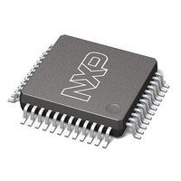
LPC11C24FBD48/301,151 NXP Semiconductors, LPC11C24FBD48/301,151 Datasheet - Page 14

LPC11C24FBD48/301,151
Manufacturer Part Number
LPC11C24FBD48/301,151
Description
Microcontrollers (MCU) CAN Transceiver MCU 32K Flash
Manufacturer
NXP Semiconductors
Datasheet
1.LPC11C22FBD48301151.pdf
(62 pages)
Specifications of LPC11C24FBD48/301,151
Processor Series
LPC11Cx4
Core
ARM Cortex-M0
Data Bus Width
32 bit
Program Memory Type
Flash
Program Memory Size
32 KB
Data Ram Size
8 KB
Interface Type
CAN, I2C, SPI, UART
Maximum Clock Frequency
50 MHz
Number Of Programmable I/os
36
Number Of Timers
4
Operating Supply Voltage
3.3 V
Maximum Operating Temperature
+ 85 C
Mounting Style
SMD/SMT
Development Tools By Supplier
OM13012,598
Minimum Operating Temperature
- 40 C
Lead Free Status / Rohs Status
Details
Other names
935294285151
NXP Semiconductors
Table 4.
[1]
[2]
[3]
[4]
[5]
[6]
[7]
LPC11CX2_CX4
Product data sheet
Symbol
GND
V
XTALIN
XTALOUT
V
DD
SS
Pin state at reset for default function: I = Input; O = Output; PU = internal pull-up enabled (pins pulled up to full V
no pull-up/down enabled.
See
reset the chip and wake up from Deep power-down mode. An external pull-up resistor is required on this pin for the Deep power-down
mode.
5 V tolerant pad providing digital I/O functions with configurable pull-up/pull-down resistors and configurable hysteresis (see
I
5 V tolerant pad providing digital I/O functions with configurable pull-up/pull-down resistors, configurable hysteresis, and analog input.
When configured as a ADC input, digital section of the pad is disabled and the pin is not 5 V tolerant (see
5 V tolerant digital I/O pad without pull-up/pull-down resistors.
When the system oscillator is not used, connect XTALIN and XTALOUT as follows: XTALIN can be left floating or can be grounded
(grounding is preferred to reduce susceptibility to noise). XTALOUT should be left floating.
2
C-bus pads compliant with the I
Figure 26
LPC11C22/C24 pin description table
for reset pad configuration. RESET functionality is not available in Deep power-down mode. Use the WAKEUP pin to
Pin
21
8; 44
6
7
5; 41
[7]
[7]
Start
logic
inputs
-
-
-
-
-
2
C-bus specification for I
Type
-
I
I
O
I
All information provided in this document is subject to legal disclaimers.
Reset
state
[1]
-
-
-
-
-
Rev. 3 — 27 June 2011
Ground for CAN transceiver.
Supply voltage to the internal regulator, the external rail, and the
Ground.
Description
ADC. Also used as the ADC reference voltage.
Input to the oscillator circuit and internal clock generator circuits.
Input voltage must not exceed 1.8 V.
Output from the oscillator amplifier.
2
C standard mode and I
2
C Fast-mode Plus.
32-bit ARM Cortex-M0 microcontroller
LPC11Cx2/Cx4
Figure
DD
© NXP B.V. 2011. All rights reserved.
25).
level); IA = inactive,
Figure
14 of 62
25).


