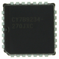
CY7B9234-270JXC Cypress Semiconductor Corp, CY7B9234-270JXC Datasheet - Page 14

CY7B9234-270JXC
Manufacturer Part Number
CY7B9234-270JXC
Description
IC TRANSMITTER HOTLINK 28-PLCC
Manufacturer
Cypress Semiconductor Corp
Series
HOTlink™r
Type
Transmitter and Receiverr
Datasheet
1.CY7B9234-270JXC.pdf
(36 pages)
Specifications of CY7B9234-270JXC
Package / Case
28-PLCC
Protocol
Fibre Channel
Voltage - Supply
4.5 V ~ 5.5 V
Mounting Type
Surface Mount
Product
PHY
Supply Voltage (min)
4.5 V
Supply Current
0.085 A
Maximum Operating Temperature
+ 70 C
Minimum Operating Temperature
0 C
Mounting Style
SMD/SMT
Number Of Channels
1
Lead Free Status / RoHS Status
Lead free / RoHS Compliant
Number Of Drivers/receivers
-
Lead Free Status / RoHS Status
Lead free / RoHS Compliant, Lead free / RoHS Compliant
Other names
428-2905-5
CY7B9234-270JXC
CY7B9234-270JXC
Available stocks
Company
Part Number
Manufacturer
Quantity
Price
Company:
Part Number:
CY7B9234-270JXC
Manufacturer:
CY
Quantity:
10
Company:
Part Number:
CY7B9234-270JXC
Manufacturer:
CYPRESS
Quantity:
831
Company:
Part Number:
CY7B9234-270JXC
Manufacturer:
Cypress Semiconductor Corp
Quantity:
10 000
Company:
Part Number:
CY7B9234-270JXCT
Manufacturer:
Cypress Semiconductor Corp
Quantity:
10 000
SMPTE HOTLink CY7B9234 Transmitter and CY7B9334 Receiver Operation
The CY7B9234 Transmitter operating with the CY7B9334
Receiver form a general purpose data communications
subsystem capable of transporting user data at up to 33Mbytes
per second (40 Mbytes per second for -400 devices) over several
types of serial interface media. Figure 2 illustrates the flow of
data through the SMPTE HOTLink CY7B9234 transmitter
pipeline. Data is latched into the transmitter on the rising edge of
CKW when enabled by ENA or ENN. RP is asserted LOW with
a 60% LOW/40% HIGH duty cycle when ENA is LOW. RP may
be used as a read strobe for accessing data stored in a FIFO.
The parallel data flows through the encoder and is then shifted
out of the OUTx± PECL drivers. The bit-rate clock is generated
internally from a multiply-by-ten PLL clock generator. The
latency through the transmitter is approximately 21t
over the operating range. A more complete description is found
in the section “CY7B9234 SMPTE HOTLink Transmitter
Operating Mode Description.”
Figure 3 illustrates the data flow through the SMPTE HOTLink
CY7B9334 receiver pipeline. Serial data is sampled by the
receiver on the INx± inputs. The receiver PLL locks onto the
serial bit stream and generates an internal bit rate clock. The bit
Document #: 38-02014 Rev. *B
D0−7,
SC/D,
SVS
OUTX
ENA
CKW
RP
±
DATA LATCHED IN
DATA
Figure 2. CY7B9234 Transmitter Data Pipeline
K28.5
TRANSMITTER LATENCY = 21 t
B
− 10 ns
stream is deserialized, decoded and then presented at the
parallel output pins. A byte rate clock (bit clock ÷ 10)
synchronous with the parallel data is presented at the CKR pin.
The RDY pin will be asserted to LOW to indicate that data or
control characters are present on the outputs. RDY will not be
asserted LOW in a field of K28.5s except for any single K28.5 or
the last one in a continuous series of K28.5’s. The latency
through the receiver is approximately 24t
operating range. A more complete description of the receiver is
in the section “CY7B9334 SMPTE HOTLink Receiver Operating
Mode Description.”
The SMPTE HOTLink Receiver has a built-in byte framer that
synchronizes the Receiver pipeline with incoming SYNC (K28.5)
characters. Figure 4 illustrates the SMPTE HOTLink CY7B9334
Receiver framing operation. The Framer is enabled when the RF
pin is asserted HIGH. RF is latched into the receiver on the falling
edge of CKR. The framer looks for K28.5 characters embedded
in the serial data stream. When a K28.5 is found, the framer sets
the parallel byte boundary for subsequent data to the K28.5
boundary. While the framer is enabled, the RDY pin indicates the
status of the framing operation.
DATA SENT
B
K28.5
− 10ns
B
+ 10 ns over the
CY7B9234
CY7B9334
DATA
Page 14 of 36
[+] Feedback


