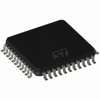
ST7538P013TR STMicroelectronics, ST7538P013TR Datasheet - Page 14

ST7538P013TR
Manufacturer Part Number
ST7538P013TR
Description
IC TXRX FSK POWER LINE 44TQFP
Manufacturer
STMicroelectronics
Type
Transceiverr
Datasheet
1.ST7538P013TR.pdf
(30 pages)
Specifications of ST7538P013TR
Number Of Drivers/receivers
1/1
Voltage - Supply
4.75 V ~ 5.25 V
Mounting Type
Surface Mount
Package / Case
44-TQFP Exposed Pad, 44-eTQFP, 44-HTQFP, 44-VQFP
For Use With
497-5484 - BOARD EVAL ST7538 PWR LINE TXRX
Lead Free Status / RoHS Status
Contains lead / RoHS non-compliant
Protocol
-
Other names
497-4316-2
Available stocks
Company
Part Number
Manufacturer
Quantity
Price
Company:
Part Number:
ST7538P013TR
Manufacturer:
NXP
Quantity:
67 000
Company:
Part Number:
ST7538P013TR
Manufacturer:
STMicroelectronics
Quantity:
10 000
ST7538
3.6 Receiving Mode
The receive section is active when
The input signal is read on RAI Pin using SGND as ground reference and then pre-filtered by a Band pass
Filter (62kHz max. bandwidth at -3dB). The Pre-Filter can be removed setting one bit in the Control Reg-
ister. The Input Stage features a wide dynamic range to receive Signal with a Very Low Signal to Noise
Ratio. The Amplitude of the applied waveform is automatically adapted by an Automatic Gain Control
block (AGC) and then filtered by a Narrow Band Band-Pass Filter centered around the Selected Channel
Frequency (14kHz max. bandwidth at -3dB). The resulting signal is down-converted by a mixer using a
sinewave generated by the FSK Modulator. Finally an Intermediate Frequency Band Pass-Filter (IF Filter)
improves the Signal to Noise ration before sending the signal to the FSK demodulator. The FSK demod-
ulator then send the signal to the RX Logic for final digital filtering. Digital filtering Removes Noise spikes
far from the BAUD rate frequency and Reduces the Signal Jitter. RxD Line is forced at logic level “0” when
neither mark or space frequencies are detected on RAI Pin.
Mark and Space Frequency in Receiving Mode must be distant at least BaudRate/2 to have a correct de-
modulation.
While ST7538 is in Receiving Mode (
are turned off. This allows the device to achieve a very low current consumption (5 mA typ). In Receiving
mode ATOP2 pin is internally connected to PAVSS.
■
■
Figure 11. ST7538 PLL lock-in range
14/30
High Sensitivity Mode
It is possible to increase ST7538 Receiving Sensitivity setting to “1” the High Sensitivity Bit of Control
Register. This Function allows to increase the communication reliability when the ST7538 sensitivity is
the limiting factor.
Synchronization Recovery System (PLL)
ST7538 embeds a Clock Recovery System to feature a Synchronous data exchange with the Host
Controller.
The clock recovery system is realized by means of a second order PLL. Data on the data line (RxD) are
stable on CLR/T line rising edge (CLR/T Falling edge synchronized to RxD line transitions ± LOCK-IN
Range).
The PLL Lock-in and Lock-out Range is ±π/2. When the PLL is in the unlock condition, CLR/T and RxD
lines are forced to a low logic level.
When PLL is in unlock condition it is sensitive to RxD Rising and Falling Edges. The maximum number
of transition required to reach the lock-in condition is 5. When in lock-in condition the PLL is sensitive
only to RxD rising Edges to reduce the CLR/T Jitter.
ST7538 PLL is forced in the un-lock condition, when more than 32 equal symbols are received.
Due to the fact that the PLL, in lock-in condition, is sensitive only to RxD rising edge, sequences equal
or longer than 15 equal symbols can put the PLL into the un-lock condition.
CLR/T
RxD
RxTx
RxTx
Pin =”1” and REG_DATA=0.
pin =”1”), the transmit circuitry, Power Line Interface included,
LOCK-IN RANGE
D03IN1417


