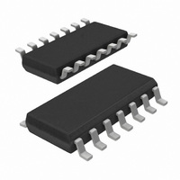
AU5790D14/N,112 NXP Semiconductors, AU5790D14/N,112 Datasheet - Page 7

AU5790D14/N,112
Manufacturer Part Number
AU5790D14/N,112
Description
IC CAN TRANSCEIVER 14-SOIC
Manufacturer
NXP Semiconductors
Series
AUr
Type
Transceiverr
Datasheet
1.AU5790D112.pdf
(20 pages)
Specifications of AU5790D14/N,112
Number Of Drivers/receivers
1/1
Protocol
CAN
Voltage - Supply
5.3 V ~ 27 V
Mounting Type
Surface Mount
Package / Case
14-SOIC (3.9mm Width), 14-SOL
Lead Free Status / RoHS Status
Lead free / RoHS Compliant
Other names
568-3054-5
935277456112
AU5790D14/N
935277456112
AU5790D14/N
Philips Semiconductors
DC CHARACTERISTICS
–40 C < T
–1 V < V
C
all voltages are referenced to pin 8 (GND); positive currents flow into the IC;
typical values reflect the approximate average value at V
2001 May 18
Pin BAT
V
V
V
I
I
I
I
I
I
I
Pin CANH
V
V
V
V
I
I
I
–I
–I
L
BATPN
BATPW
BATPH
BATN
BATW
BATH
BATS
CANHRR
CANHRD
CANHDD
BAT
BATL
BATLO
CANHN
CANHW
CANHWL
CANHH
Single wire CAN transceiver
CANH_N
CANHW
< 13.7 nF; 1 s < R
SYMBOL
CANH
amb
< +16 V; bus load resistor at pin RTH: 2 k < R
< +125 C; 5.5 V < V
Operating supply voltage
Low battery state
Supply undervoltage lockout state
Passive state supply current in
normal mode
Passive state supply current in
wake-up mode
Passive state supply current in
high speed mode
Active state supply current in
normal mode
Active state supply current in
wake-up mode
Active state supply current in
high speed mode
Sleep mode supply current
Bus output voltage in normal
mode
Bus output voltage in wake-up
mode
Bus output voltage in wake-up
mode, low battery
Bus output voltage in high-speed
transmission mode
Recessive state output current,
bus recessive
Recessive state output current,
bus dominant
Dominant state output current,
bus dominant
Bus short circuit current,
normal mode
Bus short circuit current,
wake-up mode
L
C
L
PARAMETER
< 4 s; RxD pull-up resistor 2.2 k < R
BAT
< 16 V; –0.3 V < V
Note 1
Part functional or in undervoltage
lockout state
TxD = 1 or 0; check CANH and
RxD are floating
NSTB = 5 V, EN = 5 V, TxD = 5 V
NSTB = 0 V, EN = 5 V, TxD = 5 V,
Note 2
NSTB = 5 V, EN = 0 V, TxD = 5 V,
Note 2
NSTB = 5 V, EN = 5 V, TxD = 0 V,
R
T
NSTB = 0 V, EN = 5 V, TxD = 0 V,
R
T
T
NSTB = 5 V, EN = 0 V, TxD = 0 V,
R
T
T
NSTB = 0 V, EN = 0 V, TxD = 5 V,
RxD = 5 V, –1 V < V
5.5 V < V
–40 C < T
NSTB = 5 V, EN = 5 V,
R
NSTB = 0 V, EN = 5 V,
R
NSTB = 0 V, EN = 5 V,
R
NSTB = 5 V, EN = 0 V,
R
Recessive state or sleep mode,
V
Recessive state or sleep mode,
V
TxD = 0 V, normal mode,
high-speed mode and sleep mode;
V
0 V < V
V
TxD = 0 V; NSTB = 5 V; EN = 5 V
V
TxD = 0 V; NSTB = 0 V; EN = 5 V
amb
amb
amb
amb
amb
CANH
CANH
CANH
CANH
CANH
BAT
L
L
L
L
L
L
L
TxD
= 270
= 270 , Note 2,
= 100 , Note 2,
> 270 ; 5.5 V < V
> 270 ; 11.3 V < V
> 270 ; 5.5 V < V
> 100 ; 8 V < V
= 25 C, –40 C
= 13 V and T
= 125 C
= 25 C, –40 C, Note 2
= 125 C
= 25 C, –40 C, Note 2
T
< 5.5 V; –0.3 V < V
= –1 V; 0 V < V
= 10 V; 0 V < V
= 10 V;
= –1 V,
= –1 V,
BAT
< 9.2 k ; total bus load resistance 270
BAT
CONDITIONS
j
< 16 V
< 125 C
d
T
< 14 V
< 3.0 k ; RxD: loaded with C
amb
7
= 125 C
amb
BAT
CANH
BAT
BAT
= 25 C, unless otherwise specified.
BAT
BAT
BAT
< 16 V
< 11.3 V
< 27 V
NSTB
< +1 V,
< 16 V
< 27 V
< 16 V
< 5.5 V; –0.3 V < V
V
MIN.
3.65
9.80
BAT
1.45
3.65
–10
–20
–20
5.3
2.5
30
60
LR
< 30pF to GND;
–
< R
EN
TYP.
L
< 5.5 V; –0.3 V < V
4.1
13
70
< 9.2 k ;
(V
MAX.
BAT
V
4.55
4.55
100
100
100
150
190
min
5.3
2.5
27
35
40
70
90
70
85
10
BAT
2
3
4
, 13)
AU5790
RxD
Product data
< 5.5 V;
UNIT
mA
mA
mA
mA
mA
mA
mA
mA
mA
mA
mA
V
V
V
V
V
V
V
A
A
A
A


