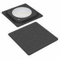
DS26519GN+ Maxim Integrated Products, DS26519GN+ Datasheet - Page 67

DS26519GN+
Manufacturer Part Number
DS26519GN+
Description
IC TXRX T1/E1/J1 16PRT 484-HSBGA
Manufacturer
Maxim Integrated Products
Type
Transceiverr
Datasheet
1.DS26519GN.pdf
(310 pages)
Specifications of DS26519GN+
Number Of Drivers/receivers
16/16
Protocol
Ethernet
Voltage - Supply
3.135 V ~ 3.465 V
Mounting Type
Surface Mount
Package / Case
484-BGA Exposed Pad, 484-eBGA, 484-HBGA
Lead Free Status / RoHS Status
Lead free / RoHS Compliant
- Current page: 67 of 310
- Download datasheet (9Mb)
9.9.4.2.6 Receive-Signaling Freeze
The signaling data in the four multiframe signaling buffers will be frozen in a known good state upon either a loss of
synchronization (OOF event), carrier loss, or change of frame alignment. In T1 mode, this action meets the
requirements of BellCore TR-TSY-000170 for signaling freezing. To allow this freeze action to occur, the RSFE
control bit (RSIGC.1) should be set high. The user can force a freeze by setting the RSFF control bit (RSIGC.2)
high. The RSIGF output pin provides a hardware indication that a freeze is in effect. The four multiframe buffer
provides a three multiframe delay in the signaling bits provided at the RSIGn pin (and at the RSERn pin if receive-
signaling reinsertion is enabled). When freezing is enabled (RSFE = 1), the signaling data will be held in the last
known good state until the corrupting error condition subsides. When the error condition subsides, the signaling
data will be held in the old state for at least an additional 9ms (4.5ms in D4 framing mode, 6ms for E1 mode) before
being allowed to be updated with new signaling data.
The receive-signaling registers are frozen and not updated during a loss of sync condition. They will contain the
most recent signaling information before the LOF occurred.
9.9.4.3 Transmit SLC-96 Operation (T1 Mode Only)
In an SLC-96-based transmission scheme, the standard Fs-bit pattern is robbed to make room for a set of
message fields. The SLC-96 multiframe is made up of six D4 superframes, hence it is 72 frames long. In the 72-
frame SLC-96 multiframe, 36 of the framing bits are the normal Ft pattern and the other 36 bits are divided into
alarm, maintenance, spoiler, and concentrator bits as well as 12-bits of the normal Fs pattern. Additional SLC-96
information can be found in BellCore document TR-TSY-000008. Registers related to the transmit FDL are shown
in
Table 9-18. Registers Related to SLC-96
Transmit FDL Register (T1TFDL)
Transmit SLC-96 Data Link Registers 1
to 3 (T1TSLC1:T1TSLC3)
Transmit Control Register 2 T1.TCR2)
Transmit Latched Status Register 1
(TLS1)
Receive SLC-96 Data Link Registers 1
to 3 (T1RSLC1:T1RSLC3)
Receive Latched Status Register 7
(RLS7)
Note: The addresses shown above are for Framer 1.
The
T1TFDL
The DS26519 will automatically insert the 12-bit alignment pattern in the Fs bits for the SLC-96 data link frame.
Data from the T1TSLC1–3 will be inserted into the remaining Fs-bit locations of the SLC-96 multiframe. The status
bit TSLC96 located at TLS1.4 will set to indicate that the SLC-96 data link buffer has been transmitted and that the
user should write new message data into T1TSLC1–3. The host will have 9ms after the assertion of TLS1.4 to write
the registers T1TSLC1–3. If no new data is provided in these registers, the previous values will be retransmitted.
Table
T1TFDL
•
•
•
•
9-18.
register, the user should configure the DS26519 as shown below:
T1.TCR2.6 (TSLC96) = 1
T1.TCR2.7 (TFDLS) = 0
TCR3.2 (TFM) = 1
TCR1.6 (TFPT) = 0
REGISTER
register is used to insert the SLC-96 message fields. To insert the SLC-96 message using the
Enable Transmit SLC-96.
Source FS bits via TFDL or SLC-96 formatter.
D4 framing mode.
Do not “pass through” TSERn F-bits.
164h, 165h, 166h
064h, 065h, 066h
ADDRESSES
FRAMER 1
162h
182h
190h
096h
67 of 310
For sending messages in transmit SLC-96 Ft/Fs
bits.
Registers that control the SLC-96 overhead
values.
Transmit control for data selection source for the
Ft/Fs bits.
Status bit for indicating transmission of data link
buffer.
—
Receive SLC-96 alignment event.
DS26519 16-Port T1/E1/J1 Transceiver
FUNCTION
Related parts for DS26519GN+
Image
Part Number
Description
Manufacturer
Datasheet
Request
R

Part Number:
Description:
Ds26519 16-port T1/e1/j1 Transceiver
Manufacturer:
Maxim Integrated Products, Inc.
Datasheet:

Part Number:
Description:
power light source LUXEON® Collimator
Manufacturer:
LUMILEDS [Lumileds Lighting Company]
Datasheet:

Part Number:
Description:
MAX7528KCWPMaxim Integrated Products [CMOS Dual 8-Bit Buffered Multiplying DACs]
Manufacturer:
Maxim Integrated Products
Datasheet:

Part Number:
Description:
Single +5V, fully integrated, 1.25Gbps laser diode driver.
Manufacturer:
Maxim Integrated Products
Datasheet:

Part Number:
Description:
Single +5V, fully integrated, 155Mbps laser diode driver.
Manufacturer:
Maxim Integrated Products
Datasheet:

Part Number:
Description:
VRD11/VRD10, K8 Rev F 2/3/4-Phase PWM Controllers with Integrated Dual MOSFET Drivers
Manufacturer:
Maxim Integrated Products
Datasheet:

Part Number:
Description:
Highly Integrated Level 2 SMBus Battery Chargers
Manufacturer:
Maxim Integrated Products
Datasheet:

Part Number:
Description:
Current Monitor and Accumulator with Integrated Sense Resistor; ; Temperature Range: -40°C to +85°C
Manufacturer:
Maxim Integrated Products

Part Number:
Description:
TSSOP 14/A°/RS-485 Transceivers with Integrated 100O/120O Termination Resis
Manufacturer:
Maxim Integrated Products

Part Number:
Description:
TSSOP 14/A°/RS-485 Transceivers with Integrated 100O/120O Termination Resis
Manufacturer:
Maxim Integrated Products

Part Number:
Description:
QFN 16/A°/AC-DC and DC-DC Peak-Current-Mode Converters with Integrated Step
Manufacturer:
Maxim Integrated Products

Part Number:
Description:
TDFN/A/65V, 1A, 600KHZ, SYNCHRONOUS STEP-DOWN REGULATOR WITH INTEGRATED SWI
Manufacturer:
Maxim Integrated Products

Part Number:
Description:
Integrated Temperature Controller f
Manufacturer:
Maxim Integrated Products

Part Number:
Description:
SOT23-6/I°/45MHz to 650MHz, Integrated IF VCOs with Differential Output
Manufacturer:
Maxim Integrated Products


