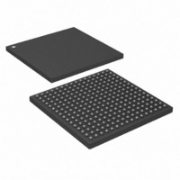
DS26528GN+ Maxim Integrated Products, DS26528GN+ Datasheet - Page 186

DS26528GN+
Manufacturer Part Number
DS26528GN+
Description
IC TXRX T1/E1/J1 OCT 256-CSBGA
Manufacturer
Maxim Integrated Products
Type
Transceiverr
Datasheet
1.DS26528G.pdf
(276 pages)
Specifications of DS26528GN+
Number Of Drivers/receivers
4/4
Protocol
IEEE 1149.1
Voltage - Supply
3.135 V ~ 3.465 V
Mounting Type
Surface Mount
Package / Case
256-CSBGA
Lead Free Status / RoHS Status
Lead free / RoHS Compliant
- Current page: 186 of 276
- Download datasheet (2Mb)
Register Name:
Register Description:
Register Address:
Bit #
Name
Default
Bits 7 to 0: Software Signaling Insertion Enable for Channels 1 to 32 (CH[1:32]). These bits determine which
channels are to have signaling inserted form the transmit-signaling registers.
Register Name:
Register Description:
Register Address:
Bit #
Name
Default
Bits 7 to 0: Per-Channel Idle Code Bits (C[7:0]). C0 is the LSB of the code (this bit is transmitted last). Address
120h is for channel 1, address 13Fh is for channel 32. TIDR1:TIDR24 are T1 mode. TIDR25:TIDR32 are E1 mode.
0 = do not source signaling data from the TS registers for this channel
1 = source signaling data from the TS registers for this channel
(MSB) 7
CH16
CH24
CH32
CH8
C7
0
7
0
CH15
CH23
CH31
SSIE1, SSIE2, SSIE3, SSIE4
Software-Signaling Insertion Enable Registers 1 to 4
118h, 119h, 11Ah, 11Bh + (200h x n): where n = 0 to 7, for Ports 1 to 8
TIDR1 to TIDR32
Transmit Idle Code Definition Registers 1 to 32
120h to 13Fh + (200h x n): where n = 0 to 7, for Ports 1 to 8
CH7
6
0
C6
6
0
CH14
CH22
CH30
CH6
5
0
C5
5
0
CH13
CH21
CH29
CH5
4
0
186 of 276
C4
4
0
CH12
CH20
CH28
CH4
3
0
C3
3
0
CH11
CH19
CH27
CH3
2
0
DS26528 Octal T1/E1/J1 Transceiver
C2
2
0
CH10
CH18
CH26
CH2
1
0
0 (LSB)
C1
CH17
CH25
1
0
CH1
CH9
0
SSIE1
SSIE2
SSIE3
SSIE4
(E1 Mode
Only)
C0
0
0
Related parts for DS26528GN+
Image
Part Number
Description
Manufacturer
Datasheet
Request
R

Part Number:
Description:
Network Controller & Processor ICs Octal E1-T1-J1 Singl e-Chip Transceiver (
Manufacturer:
Maxim Integrated Products
Datasheet:

Part Number:
Description:
Network Controller & Processor ICs Octal E1-T1-J1 Singl e-Chip Transceiver (
Manufacturer:
Maxim Integrated Products
Datasheet:

Part Number:
Description:
power light source LUXEON� Collimator
Manufacturer:
LUMILEDS [Lumileds Lighting Company]
Datasheet:

Part Number:
Description:
MAX7528KCWPMaxim Integrated Products [CMOS Dual 8-Bit Buffered Multiplying DACs]
Manufacturer:
Maxim Integrated Products
Datasheet:

Part Number:
Description:
Single +5V, fully integrated, 1.25Gbps laser diode driver.
Manufacturer:
Maxim Integrated Products
Datasheet:

Part Number:
Description:
Single +5V, fully integrated, 155Mbps laser diode driver.
Manufacturer:
Maxim Integrated Products
Datasheet:

Part Number:
Description:
VRD11/VRD10, K8 Rev F 2/3/4-Phase PWM Controllers with Integrated Dual MOSFET Drivers
Manufacturer:
Maxim Integrated Products
Datasheet:

Part Number:
Description:
Highly Integrated Level 2 SMBus Battery Chargers
Manufacturer:
Maxim Integrated Products
Datasheet:

Part Number:
Description:
Current Monitor and Accumulator with Integrated Sense Resistor; ; Temperature Range: -40°C to +85°C
Manufacturer:
Maxim Integrated Products

Part Number:
Description:
TSSOP 14/A�/RS-485 Transceivers with Integrated 100O/120O Termination Resis
Manufacturer:
Maxim Integrated Products

Part Number:
Description:
TSSOP 14/A�/RS-485 Transceivers with Integrated 100O/120O Termination Resis
Manufacturer:
Maxim Integrated Products

Part Number:
Description:
QFN 16/A�/AC-DC and DC-DC Peak-Current-Mode Converters with Integrated Step
Manufacturer:
Maxim Integrated Products

Part Number:
Description:
TDFN/A/65V, 1A, 600KHZ, SYNCHRONOUS STEP-DOWN REGULATOR WITH INTEGRATED SWI
Manufacturer:
Maxim Integrated Products

Part Number:
Description:
Integrated Temperature Controller f
Manufacturer:
Maxim Integrated Products


