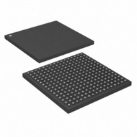
DS26528GN+ Maxim Integrated Products, DS26528GN+ Datasheet - Page 172

DS26528GN+
Manufacturer Part Number
DS26528GN+
Description
IC TXRX T1/E1/J1 OCT 256-CSBGA
Manufacturer
Maxim Integrated Products
Type
Transceiverr
Datasheet
1.DS26528G.pdf
(276 pages)
Specifications of DS26528GN+
Number Of Drivers/receivers
4/4
Protocol
IEEE 1149.1
Voltage - Supply
3.135 V ~ 3.465 V
Mounting Type
Surface Mount
Package / Case
256-CSBGA
Lead Free Status / RoHS Status
Lead free / RoHS Compliant
- Current page: 172 of 276
- Download datasheet (2Mb)
Register Name:
Register Description:
Register Address:
Bit #
Name
Default
Note: For E1 mode, see RIM7.
Bit 5: Receive RAI-CI (RRAI-CI).
Bit 4: Receive AIS-CI (RAIS-CI).
Bit 3: Receive SLC-96 (RSLC96).
Bit 2: Receive FDL Register Full (RFDLF).
Bit 1: BOC Clear Event (BC).
Bit 0: BOC Detect Event (BD).
Register Name:
Register Description:
Register Address:
Bit #
Name
Default
Note: For T1 mode, see RIM7.
Bit 1: Sa6 Codeword Detect. This bit will enable the interrupt generated when a valid codeword (per ETS 300
233) is detected in the Sa6 bits.
Bit 0: SaX Change Detect. This bit will enable the interrupt generated when a change of state is detected in any of
the unmasked SaX bit positions. The masked or unmasked SaX bits are selected by the
0 = interrupt masked
1 = interrupt enabled
0 = interrupt masked
1 = interrupt enabled
0 = interrupt masked
1 = interrupt enabled
0 = interrupt masked
1 = interrupt enabled
0 = interrupt masked
1 = interrupt enabled
0 = interrupt masked
1 = interrupt enabled
0 = interrupt masked
1 = interrupt enabled
0 = interrupt masked
1 = interrupt enabled
—
—
7
0
7
0
RIM7 (T1 Mode)
Receive Interrupt Mask Register 7 (BOC:FDL)
0A6h + (200h x n): where n = 0 to 7, for Ports 1 to 8
RIM7 (E1 Mode)
Receive Interrupt Mask Register 7 (BOC:FDL)
A6h + (200h x n): where n = 0 to 7, for Ports 1 to 8
—
—
6
0
6
0
RRAI-CI
—
5
0
5
0
RAIS-CI
172 of 276
—
4
0
4
0
RSLC96
—
3
0
3
0
DS26528 Octal T1/E1/J1 Transceiver
RFDLF
—
2
0
2
0
E1RSAIMR
Sa6CD
BC
1
0
1
0
register.
SaXCD
BD
0
0
0
0
Related parts for DS26528GN+
Image
Part Number
Description
Manufacturer
Datasheet
Request
R

Part Number:
Description:
Network Controller & Processor ICs Octal E1-T1-J1 Singl e-Chip Transceiver (
Manufacturer:
Maxim Integrated Products
Datasheet:

Part Number:
Description:
Network Controller & Processor ICs Octal E1-T1-J1 Singl e-Chip Transceiver (
Manufacturer:
Maxim Integrated Products
Datasheet:

Part Number:
Description:
power light source LUXEON� Collimator
Manufacturer:
LUMILEDS [Lumileds Lighting Company]
Datasheet:

Part Number:
Description:
MAX7528KCWPMaxim Integrated Products [CMOS Dual 8-Bit Buffered Multiplying DACs]
Manufacturer:
Maxim Integrated Products
Datasheet:

Part Number:
Description:
Single +5V, fully integrated, 1.25Gbps laser diode driver.
Manufacturer:
Maxim Integrated Products
Datasheet:

Part Number:
Description:
Single +5V, fully integrated, 155Mbps laser diode driver.
Manufacturer:
Maxim Integrated Products
Datasheet:

Part Number:
Description:
VRD11/VRD10, K8 Rev F 2/3/4-Phase PWM Controllers with Integrated Dual MOSFET Drivers
Manufacturer:
Maxim Integrated Products
Datasheet:

Part Number:
Description:
Highly Integrated Level 2 SMBus Battery Chargers
Manufacturer:
Maxim Integrated Products
Datasheet:

Part Number:
Description:
Current Monitor and Accumulator with Integrated Sense Resistor; ; Temperature Range: -40°C to +85°C
Manufacturer:
Maxim Integrated Products

Part Number:
Description:
TSSOP 14/A�/RS-485 Transceivers with Integrated 100O/120O Termination Resis
Manufacturer:
Maxim Integrated Products

Part Number:
Description:
TSSOP 14/A�/RS-485 Transceivers with Integrated 100O/120O Termination Resis
Manufacturer:
Maxim Integrated Products

Part Number:
Description:
QFN 16/A�/AC-DC and DC-DC Peak-Current-Mode Converters with Integrated Step
Manufacturer:
Maxim Integrated Products

Part Number:
Description:
TDFN/A/65V, 1A, 600KHZ, SYNCHRONOUS STEP-DOWN REGULATOR WITH INTEGRATED SWI
Manufacturer:
Maxim Integrated Products

Part Number:
Description:
Integrated Temperature Controller f
Manufacturer:
Maxim Integrated Products


