DS21348G Maxim Integrated Products, DS21348G Datasheet - Page 35
DS21348G
Manufacturer Part Number
DS21348G
Description
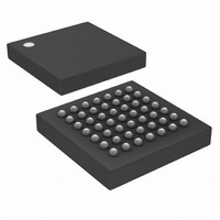
IC LIU T1/E1/J1 3.3V 49-BGA
Manufacturer
Maxim Integrated Products
Type
Line Interface Units (LIUs)r
Datasheet
1.DS21348G.pdf
(76 pages)
Specifications of DS21348G
Number Of Drivers/receivers
1/1
Protocol
T1/E1/J1
Voltage - Supply
3.135 V ~ 3.465 V
Mounting Type
Surface Mount
Package / Case
49-CSBGA
Lead Free Status / RoHS Status
Contains lead / RoHS non-compliant
Available stocks
Company
Part Number
Manufacturer
Quantity
Price

Part Number:
DS21348G
Manufacturer:
NXP/恩智浦
Quantity:
20 000
Part Number:
DS21348G+
Manufacturer:
MAXIM/美信
Quantity:
20 000
Company:
Part Number:
DS21348GN-C01
Manufacturer:
Maxim Integrated
Quantity:
10 000


SYMBOL
ARLBE
ECRS2
ECRS1
ECRS0
CCR6 (05H): COMMON CONTROL REGISTER 6
RJAB
ALB
LLB
RLB
(MSB)
LLB
POSITION DESCRIPTION
CCR6.7
CCR6.6
CCR6.5
CCR6.4
CCR6.3
CCR6.2
CCR6.1
CCR6.0
RLB
Local Loopback. In Local Loopback (LLB), transmit data will be looped back
to the receive path passing through the jitter attenuator if it is enabled. Data in
the transmit path will act as normal. See
details.
0 = loopback disabled
1 = loopback enabled
Remote Loopback. In Remote Loopback (RLB), data output from the
clock/data recovery circuitry will be looped back to the transmit path passing
through the jitter attenuator if it is enabled. Data in the receive path will act as
normal while data presented at TPOS and TNEG will be ignored.
See
0 = loopback disabled
1 = loopback enabled
Automatic Remote Loopback Enable and Reset. When this bit is set high,
the device will automatically go into remote loopback when it detects loop up
code programmed into the Receive Loop-Up Code Definition Registers
(RUPCD1 and RUPCD2) for a minimum of 5 seconds and it will also set the
RIR2.1 status bit. Once in a RLB state, it will remain in this state until it has
detected the loop code programmed into the Receive Loop-Down Code
Definition Registers (RDNCD1 and RDNCD2) for a minimum of 5 seconds at
which point it will force the device out of RLB and clear RIR2.1. The
automatic RLB circuitry can be reset by toggling this bit from a 1 to a 0. The
action of the automatic remote loopback circuitry is logically ORed with the
RLB (CCR6.6) control bit (i.e., either one can cause a RLB to occur).
Analog Loopback. In Analog Loopback (ALB), signals at TTIP and TRING
will be internally connected to RTIP and RRING. The incoming signals, from
the line, at RTIP and RRING will be ignored. The signals at TTIP and TRING
will be transmitted as normal. See
0 = loopback disabled
1 = loopback enabled
RCLK Jitter Attenuator Bypass. This control bit allows the receive recovered
clock and data to bypass the jitter attenuation while still allowing the BPCLK
output to use the jitter attenuator. See
0 = disabled
1 = enabled
Error Count Register Select 2. See Section
Error Count Register Select 1. See Section
Error Count Register Select 0. See Section
ARLBE
Figure 1-1
and Section
ALB
35 of 76
6.2.1
RJAB
for details.
Figure 1-1
Figure 1-1
Figure 1-1
ECRS2
6.4
6.4
6.4
and Section
and Section
for details.
for details.
for details.
and Section
ECRS1
6.2.3
DS21348/DS21Q348
7.3
for more details.
6.2.2
for details.
ECRS0
for
(LSB)
Related parts for DS21348G
Image
Part Number
Description
Manufacturer
Datasheet
Request
R

Part Number:
Description:
MAX7528KCWPMaxim Integrated Products [CMOS Dual 8-Bit Buffered Multiplying DACs]
Manufacturer:
Maxim Integrated Products
Datasheet:
Part Number:
Description:
Single +5V, fully integrated, 1.25Gbps laser diode driver.
Manufacturer:
Maxim Integrated Products
Datasheet:
Part Number:
Description:
Single +5V, fully integrated, 155Mbps laser diode driver.
Manufacturer:
Maxim Integrated Products
Datasheet:
Part Number:
Description:
VRD11/VRD10, K8 Rev F 2/3/4-Phase PWM Controllers with Integrated Dual MOSFET Drivers
Manufacturer:
Maxim Integrated Products
Datasheet:
Part Number:
Description:
Highly Integrated Level 2 SMBus Battery Chargers
Manufacturer:
Maxim Integrated Products
Datasheet:
Part Number:
Description:
Current Monitor and Accumulator with Integrated Sense Resistor; ; Temperature Range: -40°C to +85°C
Manufacturer:
Maxim Integrated Products
Part Number:
Description:
TSSOP 14/A�/RS-485 Transceivers with Integrated 100O/120O Termination Resis
Manufacturer:
Maxim Integrated Products
Part Number:
Description:
TSSOP 14/A�/RS-485 Transceivers with Integrated 100O/120O Termination Resis
Manufacturer:
Maxim Integrated Products
Part Number:
Description:
QFN 16/A�/AC-DC and DC-DC Peak-Current-Mode Converters with Integrated Step
Manufacturer:
Maxim Integrated Products
Part Number:
Description:
TDFN/A/65V, 1A, 600KHZ, SYNCHRONOUS STEP-DOWN REGULATOR WITH INTEGRATED SWI
Manufacturer:
Maxim Integrated Products
Part Number:
Description:
Integrated Temperature Controller f
Manufacturer:
Maxim Integrated Products
Part Number:
Description:
SOT23-6/I�/45MHz to 650MHz, Integrated IF VCOs with Differential Output
Manufacturer:
Maxim Integrated Products
Part Number:
Description:
SOT23-6/I�/45MHz to 650MHz, Integrated IF VCOs with Differential Output
Manufacturer:
Maxim Integrated Products
Part Number:
Description:
EVALUATION KIT/2.4GHZ TO 2.5GHZ 802.11G/B RF TRANSCEIVER WITH INTEGRATED PA
Manufacturer:
Maxim Integrated Products
Part Number:
Description:
QFN/E/DUAL PCIE/SATA HIGH SPEED SWITCH WITH INTEGRATED BIAS RESISTOR
Manufacturer:
Maxim Integrated Products
Datasheet: