DS21348G Maxim Integrated Products, DS21348G Datasheet - Page 14
DS21348G
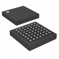
Manufacturer Part Number
DS21348G
Description
IC LIU T1/E1/J1 3.3V 49-BGA
Manufacturer
Maxim Integrated Products
Type
Line Interface Units (LIUs)r
Datasheet
1.DS21348G.pdf
(76 pages)
Specifications of DS21348G
Number Of Drivers/receivers
1/1
Protocol
T1/E1/J1
Voltage - Supply
3.135 V ~ 3.465 V
Mounting Type
Surface Mount
Package / Case
49-CSBGA
Lead Free Status / RoHS Status
Contains lead / RoHS non-compliant
Available stocks
Company
Part Number
Manufacturer
Quantity
Price

Part Number:
DS21348G
Manufacturer:
NXP/恩智浦
Quantity:
20 000
Part Number:
DS21348G+
Manufacturer:
MAXIM/美信
Quantity:
20 000
Company:
Part Number:
DS21348GN-C01
Manufacturer:
Maxim Integrated
Quantity:
10 000


2.1 Pin Descriptions
Table 2-5. Pin Descriptions in Parallel Port Mode (Sorted by Pin Name,
DS21348T Pin Numbering)
D0/AD0 to
BIS0/BIS1
ALE (AS)
A0 to A4
D7/AD7
BPCLK
NAME
MCLK
HRST
PBEO
N/A
INT
CS
19 to 12
11 to 7
32/33
PIN
31
29
23
30
—
24
4
1
I/O
I/O
O
O
O
I
I
I
I
I
I
I
Address Bus. In nonmultiplexed bus operation (BIS1 = 0, BIS0 =
1), serves as the address bus. In multiplexed bus operation (BIS1 =
0, BIS0 = 0), these pins are not used and should be tied low.
Address Latch Enable (Address Strobe). When using the parallel
port (BIS1 = 0) in multiplexed bus mode (BIS0 = 0), serves to
demultiplex the bus on a positive-going edge. In nonmultiplexed bus
mode (BIS0 = 1), should be tied low.
Bus Interface Select Bits 0 and 1. Used to select bus interface
option. See
Backplane Clock. A 16.384MHz, 8.192MHz, 4.096MHz, or
2.048MHz clock output that is referenced to RCLK selectable via
CCR5.7 and CCR5.6. In hardware mode, defaults to 16.384MHz
output.
Chip Select, Active Low. This active-low signal must be low to
read or write to the device.
Data Bus/Address/Data Bus. In nonmultiplexed bus operation
(BIS1 = 0, BIS0 = 1), serves as the data bus. In multiplexed bus
operation (BIS1 = 0, BIS0 = 0), serves as an 8-bit multiplexed
address/data bus.
Hardware Reset, Active Low. Bringing HRST low resets the
DS21348, setting all control bits to their default state of all zeros.
Interrupt, Active Low. Flags host controller during conditions and
change of conditions defined in the Status Register. Active low,
open drain output.
Master Clock. A 2.048MHz (±50ppm) clock source with TTL
levels is applied at this pin. This clock is used internally for both
clock/data recovery and for jitter attenuation. Use of a T1 1.544MHz
clock source is optional.
Not Assigned. Should be tied low.
PRBS Bit Error Output. The receiver will constantly search for a
2
Remains high if out of synchronization with the PRBS pattern. Goes
low when synchronized to the PRBS pattern. Any errors in the
received pattern after synchronization will cause a positive going
pulse (with same period as E1 or T1 clock) synchronous with
RCLK. PRBS bit errors can also be reported to the ECR1 and ECR2
registers by setting CCR6.2 to a logic 1.
15
-1 or a 2
20
Table 2-1
14 of 76
-1 PRBS depending on the ETS bit setting (CCR1.7).
for details.
FUNCTION
Related parts for DS21348G
Image
Part Number
Description
Manufacturer
Datasheet
Request
R

Part Number:
Description:
MAX7528KCWPMaxim Integrated Products [CMOS Dual 8-Bit Buffered Multiplying DACs]
Manufacturer:
Maxim Integrated Products
Datasheet:
Part Number:
Description:
Single +5V, fully integrated, 1.25Gbps laser diode driver.
Manufacturer:
Maxim Integrated Products
Datasheet:
Part Number:
Description:
Single +5V, fully integrated, 155Mbps laser diode driver.
Manufacturer:
Maxim Integrated Products
Datasheet:
Part Number:
Description:
VRD11/VRD10, K8 Rev F 2/3/4-Phase PWM Controllers with Integrated Dual MOSFET Drivers
Manufacturer:
Maxim Integrated Products
Datasheet:
Part Number:
Description:
Highly Integrated Level 2 SMBus Battery Chargers
Manufacturer:
Maxim Integrated Products
Datasheet:
Part Number:
Description:
Current Monitor and Accumulator with Integrated Sense Resistor; ; Temperature Range: -40°C to +85°C
Manufacturer:
Maxim Integrated Products
Part Number:
Description:
TSSOP 14/A�/RS-485 Transceivers with Integrated 100O/120O Termination Resis
Manufacturer:
Maxim Integrated Products
Part Number:
Description:
TSSOP 14/A�/RS-485 Transceivers with Integrated 100O/120O Termination Resis
Manufacturer:
Maxim Integrated Products
Part Number:
Description:
QFN 16/A�/AC-DC and DC-DC Peak-Current-Mode Converters with Integrated Step
Manufacturer:
Maxim Integrated Products
Part Number:
Description:
TDFN/A/65V, 1A, 600KHZ, SYNCHRONOUS STEP-DOWN REGULATOR WITH INTEGRATED SWI
Manufacturer:
Maxim Integrated Products
Part Number:
Description:
Integrated Temperature Controller f
Manufacturer:
Maxim Integrated Products
Part Number:
Description:
SOT23-6/I�/45MHz to 650MHz, Integrated IF VCOs with Differential Output
Manufacturer:
Maxim Integrated Products
Part Number:
Description:
SOT23-6/I�/45MHz to 650MHz, Integrated IF VCOs with Differential Output
Manufacturer:
Maxim Integrated Products
Part Number:
Description:
EVALUATION KIT/2.4GHZ TO 2.5GHZ 802.11G/B RF TRANSCEIVER WITH INTEGRATED PA
Manufacturer:
Maxim Integrated Products
Part Number:
Description:
QFN/E/DUAL PCIE/SATA HIGH SPEED SWITCH WITH INTEGRATED BIAS RESISTOR
Manufacturer:
Maxim Integrated Products
Datasheet: