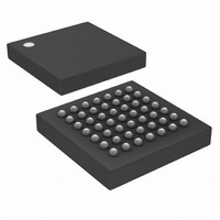
DS21348G Maxim Integrated Products, DS21348G Datasheet - Page 29

DS21348G
Manufacturer Part Number
DS21348G
Description
IC LIU T1/E1/J1 3.3V 49-BGA
Manufacturer
Maxim Integrated Products
Type
Line Interface Units (LIUs)r
Datasheet
1.DS21348G.pdf
(76 pages)
Specifications of DS21348G
Number Of Drivers/receivers
1/1
Protocol
T1/E1/J1
Voltage - Supply
3.135 V ~ 3.465 V
Mounting Type
Surface Mount
Package / Case
49-CSBGA
Lead Free Status / RoHS Status
Contains lead / RoHS non-compliant
Available stocks
Company
Part Number
Manufacturer
Quantity
Price
Part Number:
DS21348G
Manufacturer:
NXP/恩智浦
Quantity:
20 000
Part Number:
DS21348G+
Manufacturer:
MAXIM/美信
Quantity:
20 000
Company:
Part Number:
DS21348GN-C01
Manufacturer:
Maxim Integrated
Quantity:
10 000
4. CONTROL REGISTERS
CCR1 (00H): COMMON CONTROL REGISTER 1
SYMBOL
LOTCMC
(MSB)
JAMUX
RCLA
NRZE
ECUE
TTOR
ETS
TTOJ
ETS
NRZE
POSITION
CCR1.7
CCR1.6
CCR1.5
CCR1.4
CCR1.3
CCR1.2
CCR1.1
CCR1.0
RCLA
DESCRIPTION
E1/T1 Select.
0 = E1
1 = T1
NRZ Enable.
0 = Bipolar data at RPOS/RNEG and TPOS/TNEG
1 = NRZ data at RPOS and TPOS or TNEG; RNEG outputs a positive
going pulse when device receives a BPV, CV, or EXZ. See
and
Receive Carrier Loss Alternate Criteria.
0 = RCL declared upon 255 (E1) or 192 (T1) consecutive zeros
1 = RCL declared upon 2048 (E1) or 1544 (T1) consecutive zeros
Error Counter Update Enable. A 0 to 1 transition forces the next clock
cycle to load the error counter registers with the latest counts and reset
the counters. The user must wait a minimum of two clocks cycles (976ns
for E1 and 1296ns for T1) before reading the error count registers to
allow for a proper update. See Section
Jitter Attenuator MUX. Controls the source for JACLK
0 = JACLK sourced from MCLK (2.048MHz or 1.544MHz at MCLK)
1 = JACLK sourced from internal PLL (2.048MHz at MCLK)
TCLK to JACLK. Internally connects TCLK to JACLK
0 = disabled
1 = enabled
TCLK to RCLK. Internally connects TCLK to RCLK
0 = disabled
1 = enabled
Loss Of Transmit Clock Mux Control. Determines whether the
transmit logic should switch to JACLK if the TCLK input should fail to
transition
0 = do not switch to JACLK if TCLK stops
1 = switch to JACLK if TCLK stops
Figure
(Figure
ECUE
1-3.
29 of 76
1-3).
JAMUX
TTOJ
4
and
Figure 1-2
TTOR
(Figure
for details.
(Figure
(Figure
LOTCMC
Figure 1-2
1-3).
(LSB)
1-3).
1-1).


