Si5327-EVB Silicon Laboratories Inc, Si5327-EVB Datasheet - Page 52
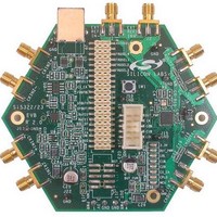
Si5327-EVB
Manufacturer Part Number
Si5327-EVB
Description
MCU, MPU & DSP Development Tools SI5327 EVAL BOARD
Manufacturer
Silicon Laboratories Inc
Specifications of Si5327-EVB
Processor To Be Evaluated
Si5327
Interface Type
I2C, SPI
Operating Supply Voltage
3.3 V
Lead Free Status / Rohs Status
Details


Si5327
52
Note: Internal register names are indicated by underlined italics, e.g., INT_PIN. See Section “5.Register Map”.
GND PAD
Pin #
29
28
34
35
36
CKOUT1+
CKOUT2+
Pin Name
CKOUT1–
CKOUT2–
CMODE
GND
GND
I/O
O
O
I
Signal Level
LVCMOS
Supply
Multi
Multi
Output Clock 1.
Differential output clock with a frequency range of 2 kHz to
808 MHz. Output signal format is selected by SFOUT1_REG regis-
ter bits. Output is differential for LVPECL, LVDS, and CML compati-
ble modes. For CMOS format, both output pins drive identical
single-ended clock outputs.
Output Clock 2.
Differential output clock with a frequency range of 2 kHz to
808 MHz. Output signal format is selected by SFOUT2_REG regis-
ter bits. Output is differential for LVPECL, LVDS, and CML compati-
ble modes. For CMOS format, both output pins drive identical
single-ended clock outputs.
Control Mode.
Selects I
0 = I
1 = SPI Control Mode
This pin must not be NC. Tie either high or low.
See the Si53xx Family Reference Manual for details on I
operation.
Ground Pad.
The ground pad must provide a low thermal and electrical
impedance to a ground plane.
Preliminary Rev. 0.4
2
C Control Mode
2
C or SPI control mode for the Si5327.
Description
2
C or SPI
Related parts for Si5327-EVB
Image
Part Number
Description
Manufacturer
Datasheet
Request
R

Part Number:
Description:
SMD/C°/SINGLE-ENDED OUTPUT SILICON OSCILLATOR
Manufacturer:
Silicon Laboratories Inc
Part Number:
Description:
Manufacturer:
Silicon Laboratories Inc
Datasheet:
Part Number:
Description:
N/A N/A/SI4010 AES KEYFOB DEMO WITH LCD RX
Manufacturer:
Silicon Laboratories Inc
Datasheet:
Part Number:
Description:
N/A N/A/SI4010 SIMPLIFIED KEY FOB DEMO WITH LED RX
Manufacturer:
Silicon Laboratories Inc
Datasheet:
Part Number:
Description:
N/A/-40 TO 85 OC/EZLINK MODULE; F930/4432 HIGH BAND (REV E/B1)
Manufacturer:
Silicon Laboratories Inc
Part Number:
Description:
EZLink Module; F930/4432 Low Band (rev e/B1)
Manufacturer:
Silicon Laboratories Inc
Part Number:
Description:
I°/4460 10 DBM RADIO TEST CARD 434 MHZ
Manufacturer:
Silicon Laboratories Inc
Part Number:
Description:
I°/4461 14 DBM RADIO TEST CARD 868 MHZ
Manufacturer:
Silicon Laboratories Inc
Part Number:
Description:
I°/4463 20 DBM RFSWITCH RADIO TEST CARD 460 MHZ
Manufacturer:
Silicon Laboratories Inc
Part Number:
Description:
I°/4463 20 DBM RADIO TEST CARD 868 MHZ
Manufacturer:
Silicon Laboratories Inc
Part Number:
Description:
I°/4463 27 DBM RADIO TEST CARD 868 MHZ
Manufacturer:
Silicon Laboratories Inc
Part Number:
Description:
I°/4463 SKYWORKS 30 DBM RADIO TEST CARD 915 MHZ
Manufacturer:
Silicon Laboratories Inc
Part Number:
Description:
N/A N/A/-40 TO 85 OC/4463 RFMD 30 DBM RADIO TEST CARD 915 MHZ
Manufacturer:
Silicon Laboratories Inc
Part Number:
Description:
I°/4463 20 DBM RADIO TEST CARD 169 MHZ
Manufacturer:
Silicon Laboratories Inc