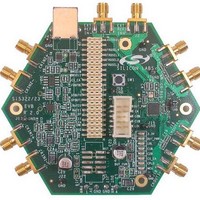
Si5327-EVB Silicon Laboratories Inc, Si5327-EVB Datasheet
Si5327-EVB
Specifications of Si5327-EVB


Related parts for Si5327-EVB

Si5327-EVB Summary of contents
Page 1
... MHz and generates two output clocks ranging from 2 kHz to 808 MHz. The two outputs are divided down separately from a common source. The Si5327 can also use its crystal oscillator as a clock source for frequency synthesis. The device provides virtually any frequency translation combination across this operating range ...
Page 2
... Si5327 Functional Block Diagram ÷ N31 CKIN1 CKIN2 ÷ N32 Xtal/Refclock Loss of Signal/ Frequency Offset Signal Detect Loss of Lock 2 Xtal or Refclock Hitless Switching Mux ® DSPLL ÷ N1_HS ÷ N2 Control 2 I C/SPI Port Clock Select Rate Select Device Interrupt Preliminary Rev. 0.4 ÷ ...
Page 3
... Typical Application Circuit . . . . . . . . . . . . . . . . . . . . . . . . . . . . . . . . . . . . . . . . . . . . . . . .18 4. Functional Description . . . . . . . . . . . . . . . . . . . . . . . . . . . . . . . . . . . . . . . . . . . . . . . . . . . 19 4.1. External Reference . . . . . . . . . . . . . . . . . . . . . . . . . . . . . . . . . . . . . . . . . . . . . . . . . . 20 4.2. Further Documentation . . . . . . . . . . . . . . . . . . . . . . . . . . . . . . . . . . . . . . . . . . . . . . . 20 5. Register Map . . . . . . . . . . . . . . . . . . . . . . . . . . . . . . . . . . . . . . . . . . . . . . . . . . . . . . . . . . . . 21 6. Register Descriptions . . . . . . . . . . . . . . . . . . . . . . . . . . . . . . . . . . . . . . . . . . . . . . . . . . . .23 7. Pin Descriptions: Si5327 . . . . . . . . . . . . . . . . . . . . . . . . . . . . . . . . . . . . . . . . . . . . . . . . . .49 8. Ordering Guide . . . . . . . . . . . . . . . . . . . . . . . . . . . . . . . . . . . . . . . . . . . . . . . . . . . . . . . . . . 54 9. Package Outline: 36-Pin QFN . . . . . . . . . . . . . . . . . . . . . . . . . . . . . . . . . . . . . . . . . . . . . . 55 10. Recommended PCB Layout . . . . . . . . . . . . . . . . . . . . . . . . . . . . . . . . . . . . . . . . . . . . . . 56 11. Si5327 Device Top Mark . . . . . . . . . . . . . . . . . . . . . . . . . . . . . . . . . . . . . . . . . . . . . . . . . 58 Document Change List . . . . . . . . . . . . . . . . . . . . . . . . . . . . . . . . . . . . . . . . . . . . . . . . . . . . .59 Contact Information ...
Page 4
... Si5327 1. Electrical Specifications Table 1. Recommended Operating Conditions Parameter Symbol Ambient Temperature T A Supply Voltage during V DD Normal Operation Note: All minimum and maximum specifications are guaranteed and apply across the recommended operating conditions. Typical values apply at nominal supply voltages and an operating temperature of 25 ºC unless otherwise stated. ...
Page 5
... CKIN See Figure 1. f > 212.5 MHz 0.25 CKIN See Figure 1. f < 212.5 MHz 0.2 CKIN See Figure 1. fCKIN > 212.5 MHz 0.25 See Figure 1. ≥ 2 Preliminary Rev. 0.4 Si5327 Typ Max Unit 251 279 mA 217 243 mA 204 234 mA 194 220 mA 165 — ...
Page 6
... Si5327 Table 2. DC Characteristics (Continued 1.8 ± 5%, 2.5 ±10%, or 3.3 V ±10 Parameter Symbol 3 Output Clocks (CKOUTn) Common Mode CKO VCM Differential Output CKO VD Swing Single Ended Output CKO VSE Swing Differential Output CKO VD Voltage Common Mode Output CKO VCM Voltage Differential Output ...
Page 7
... ICMOS[1:0] =00 — 3 1.71 V — 2.25 V — 2.97 V — 1. 2. 3.63 V 2.5 DD ≥ 2 Preliminary Rev. 0.4 Si5327 Typ Max Unit 7.5 — mA 5.5 — mA 3.5 — mA 1.75 — — — — — mA — 0.5 V — 0.7 V — 0.8 V — ...
Page 8
... Si5327 Table 2. DC Characteristics (Continued 1.8 ± 5%, 2.5 ±10%, or 3.3 V ±10 Parameter Symbol 4 3-Level Input Pins Input Voltage Low V ILL Input Voltage Mid V IMM Input Voltage High V IHH Input Low Current I ILL Input Mid Current I IMM Input High Current I IHH LVCMOS Output Pins ...
Page 9
... Output Voltage Low VOL I2C = – °C) A Test Condition Min — 0 VIN = 0 – 0 1.8V 0 2.5 or 3 1.8 V — 2.5 or 3.3 V — Preliminary Rev. 0.4 Si5327 Typ Max Unit — 0. — — 10 µA — — V — — V — 0 — 0 ...
Page 10
... Si5327 Table 3. Microprocessor Control (Continued 1.8 ± 5%, 2.5 ±10%, or 3.3 V ±10 Parameter Symbol SPI Specifications Duty Cycle, SCLK t DC Cycle Time, SCLK t c Rise Time, SCLK t r Fall Time, SCLK t f Low Time, SCLK t lsc High Time, SCLK t hsc Delay Time, SCLK Fall ...
Page 11
... See Figure 2 N1_HS 6 0.002 — Output not configured for — CMOS or Disabled See Figure 2 CMOS Output — 1. LOAD CMOS Output — 2. LOAD Preliminary Rev. 0.4 Si5327 Typ Max Unit 12 — k — 1 — 2 — 710 MHz — — — ns — ...
Page 12
... Si5327 Table 4. AC Specifications (Continued 1.8 ± 5%, 2.5 ±10%, or 3.3 V ±10 Parameter Symbol Output Duty Cycle CKO DC Uncertainty @ 622.08 MHz LVCMOS Input Pins Minimum Reset Pulse t RSTMN Width Reset to Microproces- t READY sor Access Ready Input Capacitance C in LVCMOS Output Pins Rise/Fall Times ...
Page 13
... Offset — 10 kHz Offset — 100 kHz Offset — 1 MHz Offset — Phase Noise @ 100 kHz — Offset Max spur @ — (n < 100 MHz) Preliminary Rev. 0.4 Si5327 Typ Max Unit 1000 — — s 200 — ps 0.05 0.1 dB — ...
Page 14
... Si5327 Table 5. Jitter Generation (V = 1.8 ±5%, 2.5 ±10%, or 3.3 V ±10 Parameter Symbol Test Condition Measuremen t Filter (MHz) Jitter Gen OC-48 J 0.012–20 GEN Notes MHz fundamental mode crystal used as XA/XB input 2 ° Test condition 19.44 MHz LVPECL clock output. Table 6. Thermal Characteristics (V = 1.8 ± ...
Page 15
... Exposure to absolute maximum rat- ing conditions for extended periods of time may affect device reliability. Symbol Test Condition DIG CKN VIN XA VIN T JCT T STG Preliminary Rev. 0.4 Si5327 Min Typ Max Unit –0.5 — 3.8 V –0.3 — — ...
Page 16
... Si5327 2. Typical Phase Noise Performance Figure 3. Typical Phase Noise (669.326 MHz) Jitter Bandwidth SONET_OC48, 12 kHz to 20 MHz SONET_OC192_A, 20 kHz to 80 MHz SONET_OC192_B, 4 MHz to 80 MHz SONET_OC192_C, 50 kHz to 80 MHz Brick Wall_800 MHz Note: Jitter integration bands include low-pass (–20 dB/Dec) and hi-pass (–60 dB/Dec) roll-offs per Telecordia GR-253-CORE ...
Page 17
... SONET_OC192_A, 20 kHz to 80 MHz SONET_OC192_B, 4 MHz to 80 MHz SONET_OC192_C, 50 kHz to 80 MHz Brick Wall_800 MHz Note: Jitter integration bands include low-pass (–20 dB/Dec) and hi-pass (–60 dB/Dec) roll-offs per Telecordia GR-253-CORE. Preliminary Rev. 0.4 Si5327 Jitter, RMS 329 fs 328 fs 105 fs 314 fs 339 fs ...
Page 18
... Option 1: Crystal Crystal/Ref Clk Rate Option 2: Refclk+ Refclk– Control Mode (H) Reset Figure 6. Si5327 Typical Application Circuit (SPI Control Mode) Note: For an example schematic and layout, refer to the Si5327-EVB User’s Guide µF 4 System C 0.1 µF 1 Power Ferrite ...
Page 19
... The device provides virtually any frequency translation combination across this operating range. Independent dividers are available for each input clock and output clock, so the Si5327 can accept input clocks at different frequencies and it can generate output clocks at different frequencies. The ...
Page 20
... Further Documentation Consult the Silicon Laboratories Si53xx Any Frequency Precision Clock Family Reference Manual (Si53xx FRM) for detailed information about the Si5327 functions. Additional design support is available from Silicon Laboratories through your distributor. Silicon Laboratories has developed a PC-based software utility called DSPLLsim to simplify device configuration, including frequency planning and loop bandwidth selection ...
Page 21
... CKOUT_ ALWAYS_ ON DHOLD SQ_ICAL SFOUT2_REG[2:0] HLOG_1[1:0] HIST_AVG[4:0] DSBL2_ REG VALTIME[1:0] CK2_ BAD_ PIN NC1_LS[15:8] NC1_LS[7:0] NC2_LS[15:8] NC2_LS[7:0] N2_LS[15:8] N2_LS[7:0] Preliminary Rev. 0.4 Si5327 BYPASS_ REG HIST_DEL[4:0] SFOUT1_REG[2:0] DSBL1_ REG PD_CK2 PD_CK1 LOCK[T2:0] CK1_ LOL_PIN INT_PIN BAD_ PIN CK_BAD_ LOL_POL INT_POL POL ...
Page 22
... Si5327 Register 128 129 130 DIGHOLD- VALID 131 132 134 135 PARTNUM_RO[3:0] 136 RST_REG ICAL 137 138 139 N31[15:8] N31[7:0] N32[15:8] N32[7:0] PARTNUM_RO[11:4] LOS2_EN LOS1_EN [0:0] [0:0] Preliminary Rev. 0 N31[18:16] N32[18:16] CK2_ACTV_ CK1_ACTV_ REG REG LOS2_INT LOS1_INT LOSX_INT LOL_INT LOS2_FLG LOS1_FLG ...
Page 23
... This bit enables or disables the PLL bypass mode. Use only when the device is in digital hold or before the first ICAL. 0: Normal operation 1: Bypass mode. Selected input clock is connected to CKOUT buffers, bypassing the PLL. Bypass mode does not support CMOS clock outputs. 0 Reserved CKOUT_ ALWAYS_ ON R Function Preliminary Rev. 0.4 Si5327 BYPASS_ REG R R ...
Page 24
... Si5327 Register 2. Bit D7 D6 BWSEL_REG [3:0] Name R/W Type Reset value = 0100 0010 Bit Name 7:4 BWSEL_REG BWSEL_REG. [3:0] Selects nominal f3dB bandwidth for PLL. See DSPLLsim for settings. After BWSEL_REG is written with a new value, an ICAL is required for the change to take effect. ...
Page 25
... When the output buffer is set to CMOS mode, these bits determine the output buffer drive strength. The first number below refers to 3.3 V operation; the second to 1.8 V operation. These values assume CKOUT+ is tied to CKOUT-. 00: 8mA/2mA 01: 16mA/4mA 10: 24mA/6mA 11: 32mA/8mA 5:0 Reserved HIST_DEL [4:0] R Function Function Preliminary Rev. 0.4 Si5327 R ...
Page 26
... Si5327 Register 6. Bit D7 D6 Name R R Type Reset value = 0010 1101 Bit Name 7:6 Reserved 5:3 SFOUT2_ SFOUT2_REG [2:0]. REG [2:0] Controls output signal format and disable for CKOUT2 output buffer. 000: Reserved 001: Disable 010: CMOS (Bypass mode not supported) ...
Page 27
... Reset value = 1100 0000 Bit Name 7:3 HIST_AVG HIST_AVG [4:0]. [4:0] Selects amount of averaging time to be used in generating the history information for Digital Hold. See the Si53xx Family Reference Manual for a detailed description 2:0 Reserved HLOG_1[1:0] R/W R Function R/W Function Preliminary Rev. 0.4 Si5327 ...
Page 28
... Si5327 Register 10. Bit D7 D6 Name R R Type Reset value = 0000 0000 Bit Name 7:4 Reserved 3 DSBL2_REG DSBL2_REG. This bit controls the powerdown of the CKOUT2 output buffer. If disable mode is selected, the N2_LS output divider is also powered down. 0: CKOUT2 enabled 1: CKOUT2 disabled 2 DSBL1_REG DSBL1_REG. ...
Page 29
... DSPLL. Refer to the Si53xx Family Reference Manual for more details. To minimize lock time, the value 001 for LOCKT is recommended. 000: 106 ms 001 010: 26.5 ms 011: 13.3 ms 100: 6.6 ms 101: 3.3 ms 110: 1.66 ms 111: .833 VALTIME [1:0] R R/W Function Preliminary Rev. 0.4 Si5327 LOCKT [2:0] R/W 29 ...
Page 30
... Si5327 Register 20. Bit D7 D6 Name R R Type Reset value = 0011 1110 Bit Name 7:4 Reserved 3 CK2_BAD_ CK2_BAD_PIN. PIN The CK2_BAD status can be reflected on the LOS2 output pin. 0: LOS2 output pin tristated 1: CK2_BAD status reflected to output pin 2 CK1_BAD_ CK1_BAD_PIN. PIN Either LOS1 or INT (see INT_PIN) status can be reflected on the INT_LOS1 output pin. ...
Page 31
... Sets the active polarity for the LOL status when reflected on an output pin. 0: Active low 1: Active high 0 INT_POL INT_POL. Sets the active polarity for the interrupt status when reflected on the INT_LOS1 output pin. 0: Active low 1: Active high CK_BAD_ POL Function Preliminary Rev. 0.4 Si5327 LOL_POL INT_POL R R/W R/W 31 ...
Page 32
... Si5327 Register 23. Bit D7 D6 Name R R Type Reset value = 0001 1111 Bit Name 7:3 Reserved 2 LOS2_MSK LOS2_MSK. Determines if a LOS on CKIN2 (LOS2_FLG) is used in the generation of an interrupt. Writes to this register do not change the value held in the LOS2_FLG register. 0: LOS2 alarm triggers active interrupt on INT_LOS1 output (if INT_PIN=1). ...
Page 33
... Reset value = 0000 0000 Bit Name 7:4 Reserved 3:0 NC1_LS NC1_LS [19:16]. [19:16] Sets value for NC1 low-speed divider, which drives CKOUT1 output. Must odd. 00000000000000000000 = 1 00000000000000000001 = 2 00000000000000000011 = 4 00000000000000000101 = 6 ... 11111111111111111111=2^20 Valid divider values=[ ..., 2^20 Function Function Preliminary Rev. 0.4 Si5327 NC1_LS [19:16] R/W 33 ...
Page 34
... Si5327 Register 32. Bit D7 D6 Name Type Reset value = 0000 0000 Bit Name 7:0 NC1_LS NC1_LS [15:8]. [15:8] Sets value for NC1 low-speed divider, which drives CKOUT1 output. Must odd. 00000000000000000000 = 1 00000000000000000001 = 2 00000000000000000011 = 4 00000000000000000101 = 6 ... 11111111111111111111=2^20 Valid divider values=[ ..., 2^20] Register 33. Bit D7 D6 ...
Page 35
... Reset value = 0000 0000 Bit Name 7:0 NC2_LS NC2_LS [15:8]. [15:8] Sets value for NC2 low-speed divider, which drives CKOUT2 output. Must odd. 00000000000000000000 = 1 00000000000000000001 = 2 00000000000000000011 = 4 00000000000000000101 = 6 ... 11111111111111111111=2^20 Valid divider values=[ ..., 2^20 Function NC2_LS [15:8] R/W Function Preliminary Rev. 0.4 Si5327 NC2_LS [19:16] R ...
Page 36
... Si5327 Register 36. Bit D7 D6 Name Type Reset value = 0011 0001 Bit Name 7:0 NC2_LS [7:0] NC2_LS [7:0]. Sets value for NC2 low-speed divider, which drives CKOUT2 output. Must odd. 00000000000000000000 = 1 00000000000000000001 = 2 00000000000000000011 = 4 00000000000000000101 = 6 ... 11111111111111111111=2^20 Valid divider values=[ ..., 2^20 NC2_LS [7:0] R/W Function Preliminary Rev ...
Page 37
... Sets value for N2 high speed divider, which drives N2_LS low-speed divider. 000: 4 001: 5 010: 6 011: 7 100: 8 101: 9 110: 10 111 Reserved 3:0 N2_LS [19:16] N2_LS [19:16]. Sets value for N2 low-speed divider, which drives phase detector. 00000000000000000001 = 2 00000000000000000011 = 4 00000000000000000101 = 6 ... 11111111111111111111 = 2^20 Valid divider values = [ ..., 2^20 Function Preliminary Rev. 0.4 Si5327 N2_LS [19:16] R/W 37 ...
Page 38
... Si5327 Register 41. Bit D7 D6 Name Type Reset value = 0000 0000 Bit Name 7:0 N2_LS [15:8] N2_LS [15:8]. Sets value for N2 low-speed divider, which drives phase detector. 00000000000000000001 = 2 00000000000000000011 = 4 00000000000000000101 = 6 ... 11111111111111111111 = 2^20 Valid divider values = [ ..., 2^20] Register 42. Bit D7 D6 Name Type Reset value = 1111 1001 ...
Page 39
... Valid divider values=[ ..., 2^19] Register 44. Bit D7 D6 Name Type Reset value = 0000 0000 Bit Name 7:0 N31_[15:8] N31_[15:8]. Sets value for input divider for CKIN1. 0000000000000000000 = 1 0000000000000000001 = 2 0000000000000000010 = 3 ... 1111111111111111111 = 2^19 Valid divider values=[ ..., 2^19 Function N31_[15:8] R/W Function Preliminary Rev. 0.4 Si5327 N31 [18:16] R ...
Page 40
... Si5327 Register 45. Bit D7 D6 Name Type Reset value = 0000 1001 Bit Name 7:0 N31_[7:0 N31_[7:0]. Sets value for input divider for CKIN1. 0000000000000000000 = 1 0000000000000000001 = 2 0000000000000000010 = 3 ... 1111111111111111111 = 2^19 Valid divider values=[ ..., 2^19] Register 46. Bit D7 D6 Name R Type Reset value = 0000 0000 Bit ...
Page 41
... Valid divider values=[ ..., 2^19] Register 48. Bit D7 D6 Name Type Reset value = 0000 1001 Bit Name 7:0 N32_[7:0] N32[7:0]. Sets value for input divider for CKIN1. 0000000000000000000 = 1 0000000000000000001 = 2 0000000000000000010 = 3 ... 1111111111111111111 = 2^19 Valid divider values=[ ..., 2^19 N32[15:8] R/W Function N32[7:0] R/W Function Preliminary Rev. 0.4 Si5327 ...
Page 42
... Si5327 Register 128. Bit Name Type Reset value = 0010 0000 Bit Name 7:2 Reserved 1 CK2_ACTV_REG CK2_ACTV_REG. Indicates if CKIN2 is currently the active clock for the PLL input. 0: CKIN2 is not the active input clock. Either it is not selected or LOS2_INT CKIN2 is the active input clock. ...
Page 43
... Indicates digital hold history registers have not been filled. The digital hold output frequency may not meet specifications. 1: Indicates digital hold history registers have been filled. The digital hold output frequency is valid. 5:1 Reserved 0 LOL_INT PLL Loss of Lock Status. 0: PLL locked. 1: PLL unlocked Function Preliminary Rev. 0.4 Si5327 LOL_INT ...
Page 44
... Si5327 Register 131. Bit D7 D6 Name R R Type Reset value = 0001 1111 Bit Name 7:3 Reserved 2 LOS2_FLG CKIN2 Loss-of-Signal Flag. 0: Normal operation. 1: Held version of LOS2_INT. Generates active output interrupt if output interrupt pin is enabled (INT_PIN = 1) and if not masked by LOS2_MSK bit. Flag cleared by writing 0 to this bit ...
Page 45
... LOL_MSK bit. Flag cleared by writing 0 to this bit. 0 Reserved Register 134. Bit D7 D6 Name Type Reset value = 0000 0001 Bit Name 7:0 PARTNUM_ Device 2). RO [11:0] 0000 0001 1011: Si5327 Function PARTNUM_RO [11:4] R Function Preliminary Rev. 0.4 Si5327 D2 ...
Page 46
... Register 135. Bit D7 D6 PARTNUM_RO [3:0] Name R Type Reset value = 1011 0010 Bit Name 7:4 PARTNUM_RO [11:0] Device 2). 0000 0001 1011: Si5327 3:0 REVID_RO [3:0] Device Revision. 0000: Revision A 0001: Revision B 0010: Revision C Others: Reserved Register 136. Bit D7 D6 RST_REG ICAL ...
Page 47
... Note: LOS1_EN is split between two registers. 00: Disable LOS monitoring 01: Reserved 10: Enable LOSA monitoring 11: Enable LOS monitoring LOSA is a slower and less sensitive version of LOS. See the Si53xx Family Reference Manual for details Function Function Preliminary Rev. 0.4 Si5327 FASTLOCK LOS2_EN LOS1_EN R R/W R/W 47 ...
Page 48
... Si5327 Register 139. Bit D7 D6 Name R R Type Reset value = 1111 1111 Bit Name 7:6 Reserved 5 LOS2_EN Enable CKIN2 LOS Monitoring on the Specified Input (2 of 2). Note: LOS2_EN is split between two registers. 00: Disable LOS monitoring 01: Reserved 10: Enable LOSA monitoring 11: Enable LOS monitoring LOSA is a slower and less sensitive version of LOS ...
Page 49
... Pin Descriptions: Si5327 RST NC INT_LOS1 LOS2 VDD XA XB GND NC Pin # Pin Name I/O Signal Level 1 I LVCMOS RST 2, 9, 14, NC 19, 20, 30 INT_LOS1 O LVCMOS Note: Internal register names are indicated by underlined italics, e.g., INT_PIN. See Section “5.Register Map” SDI 2 26 A2_SS ...
Page 50
... Si5327 Pin # Pin Name I/O Signal Level 4 LOS2 O LVCMOS 5, 10 Supply Analog 15, 31 GND Supply GND 11 RATE I 3-Level 16 CKIN1+ I Multi 17 CKIN1– 12 CKIN2+ I Multi 13 CKIN2– Note: Internal register names are indicated by underlined italics, e.g., INT_PIN. See Section “5.Register Map”. ...
Page 51
... In SPI control mode (CMODE = 1), this pin functions as the slave select input. This pin has a weak pull-down. Serial Data In control mode (CMODE = 0), this pin is ignored. In SPI control mode (CMODE = 1), this pin functions as the serial data input. This pin has a weak pull-down. Preliminary Rev. 0.4 Si5327 ...
Page 52
... Output is differential for LVPECL, LVDS, and CML compati- ble modes. For CMOS format, both output pins drive identical single-ended clock outputs. Control Mode. 2 Selects SPI control mode for the Si5327 Control Mode 1 = SPI Control Mode This pin must not be NC. Tie either high or low. ...
Page 53
... Table 9 lists all of the register locations that should be followed by an ICAL after their contents are changed. Table 9. Register Locations Requiring ICAL Table 10. Si5327 Internal Pull up/Pull down Addr Register 0 BYPASS_REG 0 CKOUT_ALWAYS_ON 2 BWSEL_REG 4 HIST_DEL 5 ICMOS 9 HIST_AVG 10 DSBL2_REG 10 DSBL1_REG 11 PD_CK2 11 PD_CK1 19 VALTIME 19 LOCKT ...
Page 54
... Ordering Part Output Clock Frequency Number Range Si5327B-C-GM 2 kHz–808 MHz Si5327C-C-GM 2 kHz–346 MHz Si5327D-C-GM 2 kHz–243 MHz Si5327-EVB Note: Add the end of the device to denote tape and reel options. 54 Package ROHS6, Pb-Free 36-Lead QFN 36-Lead QFN 36-Lead QFN Evaluation Board Preliminary Rev ...
Page 55
... Package Outline: 36-Pin QFN Figure 8 illustrates the package details for the Si5327. Table 11 lists the values for the dimensions shown in the illustration. Figure 8. 36-Pin Quad Flat No-lead (QFN) Symbol Millimeters Min Nom A 0.80 0.85 A1 0.00 0.02 b 0.18 0.25 D 6.00 BSC D2 3 ...
Page 56
... Si5327 10. Recommended PCB Layout Figure 10. Ground Pad Recommended Layout 56 Figure 9. PCB Land Pattern Diagram Preliminary Rev. 0.4 ...
Page 57
... The recommended card reflow profile is per the JEDEC/IPC J-STD-020 specification for Small Body Components. Preliminary Rev. 0.4 MIN MAX 0.50 BSC. 5.42 REF. 5.42 REF. 4.00 4.20 4.00 4.20 4.53 — 4.53 — — 0.28 0.89 REF. — 6.31 — 6.31 Si5327 57 ...
Page 58
... Si5327 11. Si5327 Device Top Mark Laser Mark Method: 0.80 mm Font Size: Right-Justified Si5327Q Line 1 Marking: C-GM Line 2 Marking: YYWWRF Line 3 Marking: Pin 1 Identifier Line 4 Marking: XXXX 58 Customer Part Number Q = Speed Code See Ordering Guide for options C = Product Revision G = Temperature Range – °C (RoHS6) ...
Page 59
... OCUMENT HANGE IST Revision 0.1 to Revision 0.4 Updated Table 4, “AC Specifications,” on page 11. Added table note. Updated Table 5, “Jitter Generation,” on page 14. Updated maximum jitter generation specifications. Preliminary Rev. 0.4 Si5327 59 ...
Page 60
... Si5327 C I ONTACT NFORMATION Silicon Laboratories Inc. 400 West Cesar Chavez Austin, TX 78701 Tel: 1+(512) 416-8500 Fax: 1+(512) 416-9669 Toll Free: 1+(877) 444-3032 Please visit the Silicon Labs Technical Support web page: https://www.silabs.com/support/pages/contacttechnicalsupport.aspx and register to submit a technical support request. The information in this document is believed to be accurate in all respects at the time of publication but is subject to change without notice. ...