Si5327-EVB Silicon Laboratories Inc, Si5327-EVB Datasheet
Si5327-EVB
Specifications of Si5327-EVB


Related parts for Si5327-EVB

Si5327-EVB Summary of contents
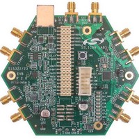
Page 1
... Si5327 EVB U SER 1. Introduction The Si5316-EVB, Si5319-EVB, Si5322/23-EVB, Si5324-EVB, Si5325/26-EVB, and Si5327-EVB provide platforms for evaluating Silicon Laboratories' Si5316, Si5319, Si5322/Si5323, Si5324, Si5325/Si5326, and Si5327 Any-Frequency Precision Clock Timing ICs. The Si5316, Si5322, and Si5323 are controlled directly using configuration pins on the devices, while the Si5319, Si5324, Si5325, Si5326, and Si5327 are controlled by a microprocessor or MCU (micro-controller unit) via an I loop bandwidth ranging from ...
Page 2
... MCU and the PC resident software that is provided with the EVB. For the MCU controlled parts (Si5319, Si5324, Si5325, Si5326, and Si5327), the devices are controlled and monitored through the serial port (either SPI or I CPLD sits between the MCU and the Any-Frequency Precision Clock device that performs voltage level translation and stores the pin configuration data for the pin controlled devices ...
Page 3
... Si5327 are for clock parts that are to be controlled by an MCU over a serial port. The Si5316-EVB, Si5319-EVB, Si5324-EVB, and Si5327-EVB support only one part, while the two other boards each support two parts: one that is wideband (the Si5322 and the Si5325) and one that is narrowband (the Si5323 and the Si5326). The narrowband parts are both capable of operating in the wideband mode, so evaluation of the wideband parts can be done by using a narrowband part in wideband mode ...
Page 4
... Reference Manual (Si53xxRM.pdf). The EVBs are shipped with a third overtone 114.285 MHz crystal that is used in the majority of applications. J1 and J2 are used when the Si532x configured in narrowband mode with an external reference oscillator (i.e. without using the 114.285 MHz crystal). The Si5327-EVB is shipped with a 40 MHz fundamental mode crystal. ...
Page 5
... RATE0 RATE1 5 RATE Notes: 1. Xtal is 114.285 MHz third overtone; 40 MHz fundamental for the Si5327-EVB 2. For external reference frequencies and RATE pin settings, see the Si53xx-RM Any-Frequency Precision Clock Family Reference Manual 3. NC—No connect. 4. NOPOP—Do not install this component. 5. RATE options for Si5327 only. ...
Page 6
Si531x-EVB Si532x-EVB +3.3 V MCU This evaluation board requires two power inputs +3.3 V for the MCU and either 1.8, 2.5, or 3.3 V for the Any-Frequency Precision Clock part. The power connector is J30. The grounds for the two ...
Page 7
Connectors and LEDs 6.1. LEDs There are eight LEDs on the board which provide a quick and convenient means of determining board status. Table 3. LED Status and Description LED Color Label D1 Green 3 Green DUT_PWR ...
Page 8
Si531x-EVB Si532x-EVB 6.2. User Jumpers and Headers Use the following to locate the jumpers described in Figure 4: Ext Ref, J1, J2 Ext Ref, J1 and 3 level 2 and 3 level Inputs, J9 Inputs, J9 Serial port, ...
Page 9
J14 pin ribbon header that provides an external path to monitor the status pins. J17 pin ribbon header that provides an external path to serially communicate with the Any-Frequency Precision Clock. To control the ...
Page 10
Si531x-EVB Si532x-EVB 7. EVB Software Installation The following sections describe how to install the EVB software. Note: These programs can control any of the Any-Frequency Precision Clock devices including the Si531x, Si532x, and Si536x devices. This software can be installed ...
Page 11
Precision Clock EVB Software Installation To install: 1. Navigate to the “PrecisionClockEVBSoftware” directory. 2. Double-click on the Setup.exe file 3. Follow the steps in the wizard to install the program. Note: Use the default installation location for best results. ...
Page 12
Si531x-EVB Si532x-EVB 8. Schematics VDD3 32 VDD2 10 VDD1 5 Rate0 11 Rate1 Rev. 0 ...
Page 13
GND 10 Vcc 20 Rev. 0.5 Si531x-EVB Si532x-EVB 13 ...
Page 14
Si531x-EVB Si532x-EVB Gnd1 2 NC2 3 NC1 1 Gnd1 2 NC2 3 NC1 1 Vcc Vss Vcc GND 6 Gnd2 Gnd2 ...
Page 15
Si531x-EVB Si532x-EVB Rev. 0.5 15 ...
Page 16
Si531x-EVB Si532x-EVB 9. Bill of Materials Item Qty Reference 1 19 C1,C2,C3,C6,C7,C8,C9,C12,C19, C20,C22,C27,C29,C32,C33,C34, C36,C39,C41 2 12 C4,C13,C14,C16,C18,C31,C35,C 37,C40,C42,C43,C44 4 7 C10,C11,C15,C21,C28,C38,C45 5 3 C17,C24,C26 6 2 C23,C25 7 3 D1,D2, D4,D5, D7, H1,H2,H3,H4 11 ...
Page 17
... Note: X denotes the product revision. Consult the ordering guide in the Si5326 data sheet for the latest product revision. For the Si5322/23-EVB, substitute Si5323A-X-GM. For the Si5316-EVB, substitute Si5316-C-GM. For the Si5319-EVB, substitute Si5319A-X-GM. For the Si5324-EVB, substitute Si5324A-X-GM. For the Si5327-EVB, substitute Si5327A-X-GM. Part Mfgr R82x4 Panasonic 113 ...
Page 18
Si531x-EVB Si532x-EVB 10. Layout 18 Figure 9. Silkscreen Top Figure 10. Layer 1 Rev. 0.5 ...
Page 19
Figure 11. Layer 2, Ground Plane Figure 12. Layer 3 Rev. 0.5 Si531x-EVB Si532x-EVB 19 ...
Page 20
Si531x-EVB Si532x-EVB 20 Figure 13. Layer 4, 3.3 V Power Figure 14. Layer 5 Rev. 0.5 ...
Page 21
Figure 15. Layer 6, DUT Power Figure 16. Layer 7, Ground Plane Rev. 0.5 Si531x-EVB Si532x-EVB 21 ...
Page 22
Si531x-EVB Si532x-EVB 22 Figure 17. Layer 8 Figure 18. Silkscreen Bottom Rev. 0.5 ...
Page 23
... A —P PPENDIX OWERUP AND For the Si5324-EVB, Si5325/26-EVB, and Si5327-EVB, the power up settings are as follows: 19.44 MHz input on CKIN1 CKIN2 is not used because of free run mode 155.52 MHz output on CKOUT1 622.08 MHz output on CKOUT2 Loop (Si5325/26-EVB) Loop (Si5324-EVB and Si5327-EVB) LVPECL outputs for CKOUT1 and CKOUT2 ...
Page 24
Si531x-EVB Si532x-EVB For the Si5316-EVB, the factory jumper settings are as follows: pin jumper — none — none FRQSEL0 L FRQSEL1 L CK1DIV L CK2DIV L BWSEL0 H BWSEL1 — none — none SFOUT0 H SFOUT1 none ...
Page 25
... Added Si5319-EVB. Add "Appendix—Powerup and Factory Default Settings" on page 23. Revision 0.2 to Revision 0.3 Updated for free run mode. Revision 0.3 to Revision 0.4 Added Si5324-EVB Revision 0.4 to Revision 0.5 Added Si5327-EVB. Changed any-rate to any-frequency. Si532x-EVB Rev. 0.5 25 ...
Page 26
... Should Buyer purchase or use Silicon Laboratories products for any such unintended or unauthorized ap- plication, Buyer shall indemnify and hold Silicon Laboratories harmless against all claims and damages. Silicon Laboratories, Silicon Labs, and DSPLL are trademarks of Silicon Laboratories Inc. Other products or brandnames mentioned herein are trademarks or registered trademarks of their respective holders. ...