MAX13342EETD+T Maxim Integrated Products, MAX13342EETD+T Datasheet - Page 7
MAX13342EETD+T
Manufacturer Part Number
MAX13342EETD+T
Description
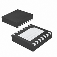
IC TXRX USB FS 3WIRE 14-TDFN
Manufacturer
Maxim Integrated Products
Type
Transceiverr
Datasheet
1.MAX13345EETDT.pdf
(18 pages)
Specifications of MAX13342EETD+T
Number Of Drivers/receivers
1/1
Protocol
USB 2.0
Voltage - Supply
2.3 V ~ 3.6 V
Mounting Type
Surface Mount
Package / Case
14-TDFN Exposed Pad
Lead Free Status / RoHS Status
Lead free / RoHS Compliant


TDFN
5, 12
EP
10
11
13
14
1
2
3
4
6
7
8
9
3-Wire Interface Full-Speed USB Transceivers
PIN
UCSP
B1
A1
A2
A3
B3
A4
B4
C4
C3
C2
B2
C1
—
—
_______________________________________________________________________________________
NAME
ENUM
V
V
GND
N.C.
DAT
SUS
SE0
BD
OE
D+
With/Without Internal Series Resistors
TRM
EP
V
D-
BUS
L
Regulated Output Voltage. V
with a 1µF (min) low-ESR capacitor, such as ceramic or plastic film types. V
to internal circuitry and the internal D+ pullup resistor. Do not use V
circuitry. These USB transceivers can also be powered by an externally regulated 3.3V supply
connected to both V
System-Side Power-Supply Input. Connect V
to GND with a 0.1µF (min) low-ESR ceramic capacitor.
Logic-Side Data Input/Output. SE0 operates as an input when OE is low and as an output when
OE is high. As an input, when SE0 is active high, D+ and D- are both driven low. As an output,
SE0 goes active high when both D+ and D- are low. (See Tables 3 and 4.)
Logic-Side Data Input/Output. DAT operates as an input for data on D+/D- when OE is low. DAT
operates as the output of the differential receiver on D+/D- when OE is high. (See Tables 3 and 4.)
No Connection. Leave N.C. unconnected. N.C. is not internally connected.
Suspend Input. Drive SUS low for normal transceiver operation. Drive SUS high for low-power
state.
USB Detector Output. A high on BD indicates that V
Output Enable. OE controls the USB transmitter outputs (D+/D-) and the interface signals (DAT,
SE0) when in USB mode. Drive OE high to operate D+/D- as inputs and to operate the logic
interface signals as outputs. Drive OE low to operate D+/D- as outputs and to operate the logic
interface signals as inputs.
Ground
Negative USB Differential Data Input/Output. D- is wired to the USB connector directly
(MAX13345E) or through a series resistor (MAX13342E). D- operates as an input when OE is high
and as an output when OE is low.
Positive USB Differential Data Input/Output. D+ is wired to the USB connector directly
(MAX13345E) or through a series resistor (MAX13342E). D+ operates as an input when OE is
high and as an output when OE is low.
Enumerate. Drive ENUM high to connect the internal 1.5kΩ resistor from D+ to V
low to disconnect the internal 1.5kΩ resistor.
USB-Side Power-Supply Input. Connect V
GND with a 1µF ceramic capacitor.
Exposed Paddle. Connect EP to GND.
BUS
and V
TRM
TRM.
provides a 3.3V output derived from V
BUS
FUNCTION
L
to the systems logic-level power supply. Bypass V
to the incoming USB power supply. Bypass V
BUS
is present.
TRM
Pin Description
BUS
to power external
. Bypass V
TRM
provides power
TRM
. Drive ENUM
TRM
to GND
BUS
to
L
7
Related parts for MAX13342EETD+T
Image
Part Number
Description
Manufacturer
Datasheet
Request
R

Part Number:
Description:
(MAX13342E / MAX13345E) 3-Wire Interface Full Speed USB Transceivers
Manufacturer:
Maxim Integrated Products
Datasheet:

Part Number:
Description:
3 Digit DMM Circuit
Manufacturer:
Maxim
Datasheet:
Part Number:
Description:
Data Conversion IC Development Tools Evaluation Kit for the MAX134
Manufacturer:
Maxim Integrated
Datasheet:
Part Number:
Description:
Data Conversion IC Development Tools
Manufacturer:
Maxim Integrated
Datasheet:
Part Number:
Description:
Data Conversion IC Development Tools
Manufacturer:
Maxim Integrated
Datasheet:
Part Number:
Description:
MAX7528KCWPMaxim Integrated Products [CMOS Dual 8-Bit Buffered Multiplying DACs]
Manufacturer:
Maxim Integrated Products
Datasheet:
Part Number:
Description:
Single +5V, fully integrated, 1.25Gbps laser diode driver.
Manufacturer:
Maxim Integrated Products
Datasheet:
Part Number:
Description:
Single +5V, fully integrated, 155Mbps laser diode driver.
Manufacturer:
Maxim Integrated Products
Datasheet:
Part Number:
Description:
VRD11/VRD10, K8 Rev F 2/3/4-Phase PWM Controllers with Integrated Dual MOSFET Drivers
Manufacturer:
Maxim Integrated Products
Datasheet:
Part Number:
Description:
Highly Integrated Level 2 SMBus Battery Chargers
Manufacturer:
Maxim Integrated Products
Datasheet:
Part Number:
Description:
Current Monitor and Accumulator with Integrated Sense Resistor; ; Temperature Range: -40°C to +85°C
Manufacturer:
Maxim Integrated Products
Part Number:
Description:
TSSOP 14/A�/RS-485 Transceivers with Integrated 100O/120O Termination Resis
Manufacturer:
Maxim Integrated Products
Part Number:
Description:
TSSOP 14/A�/RS-485 Transceivers with Integrated 100O/120O Termination Resis
Manufacturer:
Maxim Integrated Products
Part Number:
Description:
QFN 16/A�/AC-DC and DC-DC Peak-Current-Mode Converters with Integrated Step
Manufacturer:
Maxim Integrated Products
Part Number:
Description:
TDFN/A/65V, 1A, 600KHZ, SYNCHRONOUS STEP-DOWN REGULATOR WITH INTEGRATED SWI
Manufacturer:
Maxim Integrated Products