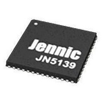
JN5148/001,531 NXP Semiconductors, JN5148/001,531 Datasheet - Page 39

JN5148/001,531
Manufacturer Part Number
JN5148/001,531
Description
Microcontrollers (MCU) 32bit RISC 2.4GHz
Manufacturer
NXP Semiconductors
Datasheet
1.JN5148001531.pdf
(99 pages)
Specifications of JN5148/001,531
Core
RISC
Operating Supply Voltage
2 V to 3.6 V
Maximum Operating Temperature
+ 85 C
Mounting Style
SMD/SMT
Package / Case
QFN-56
Minimum Operating Temperature
- 40 C
Lead Free Status / Rohs Status
Details
The clock source for the timer unit is fed from the 16MHz system clock. This clock passes to a 5-bit prescaler where a
prescale
value of 0 leaves the clock unmodified and other values divide it by 2
value. For example, a prescale value of
2 applied to the 16MHz system clock source results in a timer clock of 4MHz.
The counter is optionally gated by a signal on the clock/gate input (TIMxCK_GT). If the gate function is selected,
then the counter is frozen when the clock/gate input is high.
An interrupt can be generated whenever the counter is equal to the value in either of the High or Low registers.
The internal Output Enable (OE) signal enables or disables the timer output.
The Timer 0 signals CK_GT, CAP and OUT are alternate functions of pins DIO8, 9 and 10 respectively and Timer 1
signals CK_GT, CAP and OUT are alternate functions of pins DIO11, 12, and 13 respectively. Timer 2 OUT is an
alternate function of DIO11 If operating in timer mode it is not necessary to use any of the DIO pins, allowing the
standard DIO functionality to be available to the application.
Note, timer 0 may only be used as an internal timer or in counter mode (counting events) if an external 32kHz crystal
is used. If timer 2 is used in PWM or Delta-Sigma mode then timer 1 does not have access to its clock/gate pin.
Therefore, it can not operate in counter mode (counting events) or use the gate function.
11.1.1 Pulse Width Modulation Mode
Pulse Width Modulation (PWM) mode allows the user to specify an overall cycle time and pulse length within the
cycle. The pulse can be generated either as a single shot or as a train of pulses with a repetition rate determined by
the cycle time.
In this mode, the cycle time and low periods of the PWM output signal can be set by the values of two independent
16-bit registers (Fall and Rise). The counter increments and its output is compared to the 16-bit Rise and Fall
registers. When the counter is equal to the Rise register, the PWM output is set to high; when the counter reaches
the Fall value, the output returns to low. In continuous mode, when the counter reaches the Fall value, it will reset
and the cycle repeats. The PWM waveform is available on TIMxOUT when the output driver is enabled.
Rise
Fall
Figure 27: PWM Output Timings
11.1.2 Capture Mode
The capture mode can be used to measure the time between transitions of a signal applied to the capture input
(TIMxCAP). When the capture is started, on the next low-to-high transition of the captured signal, the count value is
stored in the Rise register, and on the following high-to-low transition, the counter value is stored in the Fall register.
The pulse width is the difference in counts in the two registers multiplied by the period of the prescaled clock. Upon
reading the capture registers the counter is stopped. The values in the High and Low registers will be updated
whenever there is a corresponding transition on the capture input, and the value stored will be relative to when the
mode was started. Therefore, if multiple pulses are seen on TIMxCAP before the counter is stopped only the last
pulse width will be stored.
© NXP Laboratories UK 2010
JN-DS-JN5148-001 1v6
39


