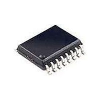
HV9123NG Supertex, HV9123NG Datasheet - Page 6

HV9123NG
Manufacturer Part Number
HV9123NG
Description
Switching Converters, Regulators & Controllers HVCMOS 450V 2% Ref
Manufacturer
Supertex
Datasheet
1.HV9123P-G.pdf
(11 pages)
Specifications of HV9123NG
Output Voltage
4.08 V
Mounting Style
SMD/SMT
Package / Case
SOIC-16
Lead Free Status / Rohs Status
Lead free / RoHS Compliant
Available stocks
Company
Part Number
Manufacturer
Quantity
Price
Part Number:
HV9123NG
Manufacturer:
SUPERTEX
Quantity:
20 000
(reference output pin and non-inverting input to the error
amplifier). This allows overriding the internal reference with
a low-impedance voltage source ≤6.0V. Using an external
reference reinstates the input offset voltage of the error am-
plifier, and its effect of the exact value of feedback voltage
required. In general, because the reference voltage of the
Supertex HV9123 is not noisy, as some previous examples
have been, overriding the reference should seldom be nec-
essary.
Because the reference of the HV9123 is a high impedance
node, and usually there will be significant electrical noise
near it, a bypass capacitor between the reference pin and
VSS is strongly recommended. The reference buffer ampli-
fier is intentionally compensated to be stable with a capaci-
tive load of 0.01 to 0.1µF.
Error Amplifier
The error amplifier in the HV9123 is a true low-power dif-
ferential input operational amplifier intended for around-the-
amplifier compensation. It is of mixed CMOS-bipolar con-
struction: A PMOS input stage is used so the common-mode
range includes ground and the input impedance is very high.
This is followed by bipolar gain stages which provide high
gain without the electrical noise of all-MOS amplifiers. The
amplifier is unity-gain stable.
Truth Table
Shutdown Timing Waveforms
SHUTDOWN
L → H
H
H
L
L
SHUTDOWN
OUTPUT
SENSE
RESET
VDD
1.5V
0
0
VDD
VDD
RESET
H → L
0
0
H
H
L
L
50%
●
50%
1235 Bordeaux Drive, Sunnyvale, CA 94089
t
d
Output
Normal operation
Normal operation, no change
Off, not latched
Off, latched
Off, latched, no change
90%
t
R
≤ 10ns
50%
t
SW
t
LW
6
Current Sense Comparators
The HV9123 uses a true dual-comparator system with in-
dependent comparators for modulation and current limiting.
This allows the designer greater latitude in compensation
design, as there are no clamps (except ESD protection) on
the compensation pin. Like the error amplifier, the compara-
tors are of low-noise BiCMOS construction.
Remote Shutdown
The SHUTDOWN and RESET pins of the HV9123 can be
used to perform either latching or non-latching shutdown of
a converter as required. These pins have internal current
source pull-ups so they can be driven from open-drain logic.
When not used, they should be left open, or connected to
VDD.
Output Buffer
The output buffer of the HV9123 is of standard CMOS con-
struction (P-channel pull-up, N-channel pull-down). Thus the
body-drain diodes of the output stage can be used for spike
clipping if necessary, and external Schottky diode clamping
of the output is not required.
50%
SHUTDOWN
OUTPUT
50%
●
VDD
VDD
Tel: 408-222-8888
0
0
t
RW
50%
50%
t
SD
●
www.supertex.com
90%
t
R
, t
t
F
F
≤ 10ns
≤ 10ns
HV9123


