HV7022DJ-C Supertex, HV7022DJ-C Datasheet

MOSFET & Power Driver ICs 34-Ch Conv

HV7022DJ-C

Manufacturer Part Number
HV7022DJ-C
Description
MOSFET & Power Driver ICs 34-Ch Conv
Manufacturer
Supertex
Type
Symmetric Row Driverr
Datasheet

Specifications of HV7022DJ-C

Product
Driver ICs - Various
Supply Current
10 mA
Maximum Operating Temperature
+ 125 C
Mounting Style
SMD/SMT
Package / Case
CLCC-44
Minimum Operating Temperature
- 55 C
Lead Free Status / Rohs Status
Lead free / RoHS Compliant
*For Hi-Rel process flows, refer to page 5-3 of the databook.
Features
❏ Processed with HVCMOS
❏ Symmetric row drive (reduces latent imaging
❏ Output voltages up to 230V
❏ Low-power level shifting
❏ Source/Sink current 70mA (min.)
❏ Shift register speed 4MHz
❏ Pin-programmable shift direction
❏ 44-lead plastic & ceramic surface-mount packages
❏ Hi-Rel processing available
Absolute Maximum Ratings
Supply voltage, V
Supply voltage, V
Logic input levels
Ground current
Continuous total power dissipation
Operating temperature range
Storage temperature range
Lead temperature 1.6mm (1/16 inch)
from case for 10 seconds
Notes:
1. All voltages are referenced to GND.
2. Duty cycle is limited by the total power dissipated in the package.
3. For operation above 25°C ambient derate linearly to maximum operating
02/96/022
Supertex Inc. does not recommend the use of its products in life support applications and will not knowingly sell its products for use in such applications unless it receives an adequate "products liability
indemnification insurance agreement." Supertex does not assume responsibility for use of devices described and limits its liability to the replacement of devices determined to be defective due to
workmanship. No responsibility is assumed for possible omissions or inaccuracies. Circuitry and specifications are subject to change without notice. For the latest product specifications, refer to the
Supertex website: http://www.supertex.com. For complete liability information on all Supertex products, refer to the most current databook or to the Legal/Disclaimer page on the Supertex website.
Ordering Information
HV7022-C
Device
temperature at 25mW/°C for plastic and at 15mW/°C for ceramic.
in ACTFEL displays)
2
Ceramic Chip Carrier
1
DD
PP
44 J-Lead Quad
1
1
HV7022DJ-C
®
technology
34-Channel Symmetric Row Driver
Plastic
Ceramic
3
:
Plastic
Ceramic
-0.3V to V
-65°C to +150°C
Plastic Chip Carrier
-40°C to +85°C
-55°C to 125°C
-0.3V to +250V
-0.3V to +15V
44 J-Lead Quad
HV7022PJ-C
1200mW
1500mW
DD
260°C
+0.3V
1.5A
Package Options
1
General Description
The HV7022-C is a low-voltage serial to high-voltage parallel
converter with push-pull outputs. It is especially suited for use as
a symmetric row driver in AC thin-film electroluminescent (ACTFEL)
displays. The HV70 offers 34 output lines, a direction (DIR) pin to
give CW or CCW shift register loading, output enable (OE), and
polarity (POL) control. After DATA INPUT is entered (on the falling
edge of CLOCK), a logic high will cause the output to swing to V
if POL is high, or to GND if POL is low.
For Detailed circuit and application information, please refer
to Application Note AN-H3.
waffle pack
HV7022X-C
Die in
(MIL-Std-883 Processed*)
Ceramic Chip Carrier
HV7022-C
44 J-Lead Quad
RBHV7022DJ-C
PP

Related parts for HV7022DJ-C

HV7022DJ-C Summary of contents

Page 1

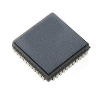
... Plastic 1200mW Ceramic 1500mW -40°C to +85°C -55°C to 125°C -65°C to +150°C 260°C For Detailed circuit and application information, please refer to Application Note AN-H3. 1 HV7022-C Die in 44 J-Lead Quad waffle pack Ceramic Chip Carrier (MIL-Std-883 Processed*) HV7022X-C RBHV7022DJ-C PP ...

Page 2

Electrical Characteristics (over recommended operating conditions Characteristics Symbol Parameter I V supply current High voltage supply current PP I Quiescent V supply current DDQ DD V High-level output OH V Low-level output OL I ...

Page 3

Recommended Operating Conditions Symbol V Logic supply voltage DD V High voltage supply PP V High-level input voltage IH V Low-level input voltage IL f Clock frequency CLK T Operating free-air temperature A I Allowable pulse current through output diodes ...

Page 4

Switching Waveforms Clock 50% t SUD 50% Data Input Data Output ( IOA IOB SUC GND POL GND 50 OUT High Impedance HV OUT l/f CLK ...

Page 5

Functional Block Diagram Polarity V DD Data In CLK DIR Data Out Function Table I/O CLK Relations O/P HIGH X O/P OFF X O/P LOW X O/P OFF X O/P OFF X ↓ Load S/R, ↓ set ...

Page 6

... HV 20 Output Enable Clock GND 44 HV Note: Pin designation for DIR L/H Example:For DIR = L, pin OUT For DIR = H, pin OUT ©2002 Supertex Inc. All rights reserved. Unauthorized use or reproduction prohibited. Temp = 25 C ° 100 Package Outline DD PP 34/1 OUT 33/2 OUT ...

Page 7

PQFP Package Outline (PG) Note 1 (Index Area D1/4 x E1/ Top View Side View Note 1: A Pin 1 identifi er must be located in the index area indicated. The Pin 1 ...

Page 8

PLCC Package Outline (PJ) .653x.653in body, .180in height (max.), .050in pitch .048/.042 .150 MAX .075 MAX Note 2 (3 places) 0.20max 3 Places Note Pin 1 identifi er must ...

Related keywords