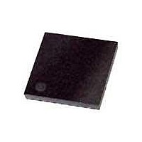
HV746K6-G Supertex, HV746K6-G Datasheet

HV746K6-G
Specifications of HV746K6-G
Related parts for HV746K6-G
HV746K6-G Summary of contents
Page 1
... Supertex inc. Dual, High Speed, General Description The Supertex HV746 is a dual-channel monolithic high voltage high- speed pulse generator designed for portable medical ultrasound applications. This high voltage and high-speed integrated circuit can also be used for other piezoelectric, capacitive or MEMS sensor in ultrasonic nondestructive detection and sonar ranger applications ...
Page 2
... V with logic signal low – Logic control signals Supertex inc. 48-Lead QFN 0.50mm pitch HV746K6-G Value 0V -0.5V to +7.0V -0.5V to +14V -0.5V to +14V -0.5V to +14V +170V -0.5V to +85V +0.5V to –85V -0.5V to +7.0V -0.5V to +7.0V +170V +170V +170V +170V -40°C to 125°C -65°C to 150°C 29° ...
Page 3
... V V threshold UVLL threshold UVVF OTP flag output low voltage OL_OTP I Max. open drain output current OTP T Over temperature threshold OTP T OTP output reset hysteresis HYS Supertex inc +3.3V +9.0V Min Typ 1.2 1.8 to 3.3 8.0 9.0 (V -12) (V -9. +8.0) (V +9. ...
Page 4
... EN t Disable time DIS t Delay time on inputs rise dr t Delay time on inputs fall df Δt Delay time matching delay t Delay on mode change dm t Delay jitter on rise or fall J * Guaranteed by design. Supertex inc. ● +3.3V +9.0V Min Typ 2.5 3.6 - 4.0 - 200* Min Typ 2 ...
Page 5
... Switch AC Test Timing Diagram NINx PINx Output V OTP EN EN_PWR MC0 MC1 PIN1 NIN1 PINx TXPx Supertex inc. 90 10 SUB DD SUB Level P-Driver Translator Level N-Driver Translator 1of n Channels GREF VSS V 50% NINx t dfp t drp I t OUT drn 50% 0A TXNx 0A ● ...
Page 6
... Input logic control of high voltage output P-FET of channel ON, Low = OFF. 10 NIN2 Input logic control of high voltage output N-FET of channel ON, Low = OFF. 11 VSS Power supply return (0V). 12 VDD Positive internal voltage supply (+9.0V). 13 OTP Over temperature protection output, open N-FET drain, active low if IC temperature >110°C. Supertex inc. PIN NIN ...
Page 7
... GREF Logic low reference, logic ground (0V). 48 VLL Logic Hi voltage reference input (+3.3V). Thermal Pad Substrate bottom is internally connected to the central thermal pad on the bottom of package. It (VSUB) must be connected to VSUB, the most positive potential of the IC externally. Supertex inc ● 1235 Bordeaux Drive, Sunnyvale, CA 94089 ...
Page 8
... This dimension is not specified in the JEDEC drawing. † This dimension differs from the JEDEC drawing. Drawings are not to scale. Supertex Doc.#: DSPD-48QFNK67X7P050, Version C041009. (The package drawing(s) in this data sheet may not reflect the most current specifications. For the latest package outline information go to http://www.supertex.com/packaging.html.) does not recommend the use of its products in life support applications, and will not knowingly sell them for use in such applications unless it receives Supertex inc ...


