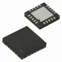
ATA6621N-PGPW Atmel, ATA6621N-PGPW Datasheet - Page 12

ATA6621N-PGPW
Manufacturer Part Number
ATA6621N-PGPW
Description
TXRX LIN 5V REG WATCHDOG 20-QFN
Manufacturer
Atmel
Type
Transceiverr
Datasheet
1.ATA6621N-PGPW.pdf
(28 pages)
Specifications of ATA6621N-PGPW
Number Of Drivers/receivers
1/1
Protocol
LIN
Voltage - Supply
5 V ~ 18 V
Mounting Type
Surface Mount
Package / Case
20-QFN Exposed Pad
Number Of Transmitters
1
Number Of Receivers
1
Power Supply Requirement
Single
Package Type
QFN EP
Operating Temperature Classification
Automotive
Mounting
Surface Mount
Pin Count
20
Operating Temperature (max)
125C
Operating Temperature (min)
-40C
Dual Supply Voltage (typ)
Not RequiredV
Dual Supply Voltage (max)
Not RequiredV
Dual Supply Voltage (min)
Not RequiredV
Lead Free Status / RoHS Status
Lead free / RoHS Compliant
3.17
12
Fail-safe Features
ATA6621N
Figure 3-6.
• During a short circuit at LIN, the output limits the output current to I
• The reverse current at pin LIN is very low (< 3 µA) during loss of V
• During a short circuit at V
• Pin EN provides a pull-down resistor to force the transceiver into recessive mode if EN is
• Pin RXD is connected with 5 k to V
• Pin TXD provides a pull-up resistor to force the transceiver into recessive mode if TXD is
LIN Bus
dissipation, the chip temperature exceeds T
cools down and after a hysteresis of T
overtemperature switch-off, the V
behavior for bus systems where some slave modes are supplied from battery or ignition.
undervoltage, NRES switches to low and sends a reset to the microcontroller. The IC
switches into Pre-normal mode. If the chip temperature exceeds the value T
output switches off. The chip cools down and after a hysteresis of T
again. Because of Pre-normal mode, the V
switched off from the microcontroller. The microcontroller can start its normal operation.
disconnected.
disconnected.
NRES
RXD
VCC
TXD
EN
If undervoltage, switch to Pre-normal Mode
Node in Silent mode
Wake Up from Sleep/Silent Mode at an Insufficient Falling Edge at Pin LIN
Wake-up filtering time
VLIN < V
VLIN > 0.6 V
Silent mode
High
High
CC
t
WAKE
, the output limits the output current to I
S
- 1V and
S
CC
Regulator Wake-up time
regulator works independently.
CC
hys
, if V
, switches the output on again. During LIN
CC
Batt
LINoff
voltage will switch on again although EN is
is disconnected V
and the LIN output is switched off. The chip
Pre-normal Mode
Pre-normal mode
Undervoltage detection active
Low
Low
CC
BAT
hys
BUS_LIM
VCCn
is at GND level
, switches the output on
or GND. This is optimal
. Because of
. Due to the power
VCCoff
Normal mode
Normal Mode
4887I–AUTO–09/09
EN High
, the V
CC


