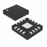
MAX3984UTE+ Maxim Integrated Products, MAX3984UTE+ Datasheet - Page 14

MAX3984UTE+
Manufacturer Part Number
MAX3984UTE+
Description
IC PREMP DRIVER 1CH 16-TQFN
Manufacturer
Maxim Integrated Products
Type
Driverr
Specifications of MAX3984UTE+
Number Of Drivers/receivers
1/0
Protocol
Ethernet
Voltage - Supply
3 V ~ 3.6 V
Mounting Type
Surface Mount
Package / Case
16-TQFN Exposed Pad
Lead Free Status / RoHS Status
Lead free / RoHS Compliant
1Gbps to 10Gbps Preemphasis Driver with
Receive Equalizer
Circuit board layout and design can significantly affect
the performance of the MAX3984. Use good high-fre-
quency design techniques, including minimizing
ground inductance and using controlled-impedance
transmission lines on the data signals. Power-supply
decoupling should also be placed as close as possible
to the V
power plane. Take care to isolate the input from the
output signals to reduce feed through.
Figure 5. IN+/IN- Equivalent Input Structure
Figure 6. OUT+/OUT- Equivalent Output Structure
14
______________________________________________________________________________________
IN+
IN-
CC
pins. Always connect all V
50Ω
V
V
CC2
CC1
V
50Ω
CC1
50Ω
GND
GND
- 1.5V
Layout Considerations
50Ω
CC
OUT+
OUT-
pins to a
The exposed-pad, 16-pin thin QFN package incorpo-
rates features that provide a very low thermal resis-
tance path for heat removal from the IC. The exposed
pad on the MAX3984 must be soldered to the circuit
board for proper thermal performance. Refer to Maxim
Application Note HFAN-08.1: Thermal Considerations
of QFN and Other Exposed-Paddle Packages for addi-
tional information.
Figure 7. LVTTL Equivalent Input Structure
Figure 8. Loss-of-Signal Equivalent Output Structure
LVTTL IN
IN_LEV
OUT_LEV
TX_DISABLE, PE0, PE1
PIN NAME
Interface Schematics
Exposed-Pad Package
R
PULLUP
V
V
V
V
CCX
CC1
CC2
CC2
GND
V
GND
CCX
R
PULLUP
40
20
10
(kΩ)
LOS


