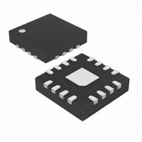
MAX3984UTE+ Maxim Integrated Products, MAX3984UTE+ Datasheet

MAX3984UTE+
Specifications of MAX3984UTE+
Related parts for MAX3984UTE+
MAX3984UTE+ Summary of contents
Page 1
... Output Swing ♦ Selectable Output Preemphasis ♦ Selectable Input Equalization ♦ LOS Detection with Built-In Squelch ♦ Transmit Disable ♦ Hot Pluggable Applications PART MAX3984UTE+ + Denotes a lead-free package. *EP = Exposed pad. ACTIVE CABLE ASSEMBLY ≤ 10m (24 AWG 10Gbps LOS 39Ω COPPER CABLE DIFFERENTIAL 100Ω ...
Page 2
Preemphasis Driver with Receive Equalizer ABSOLUTE MAXIMUM RATINGS Supply Voltage Range (V ).................................-0.5V to +4.1V CC Continuous Output Current Range (OUT+, OUT-) ...............................................-25mA to +25mA Input Voltage Range (IN+, IN-) ..................-0. Stresses beyond those listed ...
Page 3
Preemphasis Driver with ELECTRICAL CHARACTERISTICS (V = +3.0V to +3.6V 0°C to +85°C. Typical values are PARAMETER SYMBOL Supply Current I Inrush Current Power-On Delay EQUALIZER AND DRIVE SPECIFICATIONS Input Return ...
Page 4
Preemphasis Driver with Receive Equalizer ELECTRICAL CHARACTERISTICS (continued +3.0V to +3.6V 0°C to +85°C. Typical values are PARAMETER SYMBOL Residual Output Deterministic Jitter at 5.0Gbps (Notes 4, 8, and ...
Page 5
Preemphasis Driver with ELECTRICAL CHARACTERISTICS (continued +3.0V to +3.6V 0°C to +85°C. Typical values are PARAMETER SYMBOL LOS Open-Collector Current Sink LOS Response Time (Note 4) LOS Transition Time ...
Page 6
Preemphasis Driver with Receive Equalizer Figure 1. TX Preemphasis SIGNAL SOURCE SMA CONNECTORS OSCILLOSCOPE OR ERROR DETECTOR D Figure 2. Transmit Test Setup (The points labeled A, B, and D are referenced for AC ...
Page 7
Preemphasis Driver with A SIGNAL SOURCE SMA CONNECTORS Figure 3. Receive-Side Test Setup (The points labeled A and D are referenced for AC parameter tests +3.3V +25°C, PRBS7 + 100 CID pattern is ...
Page 8
Preemphasis Driver with Receive Equalizer (V = +3.3V +25°C, PRBS7 + 100 CID pattern is PRBS FR-4 at the input, IN_LEV = high, 360mV DETERMINISTIC JITTER vs. FR-4 LENGTH (10.3Gbps) 1.0 ...
Page 9
Preemphasis Driver with (V = +3.3V +25°C, PRBS7 + 100 CID pattern is PRBS FR-4 at the input, IN_LEV = high, 360mV VERTICAL EYE OPENING vs. FR-4 LENGTH (10.3Gbps) 700 IN_LEV ...
Page 10
Preemphasis Driver with Receive Equalizer PIN NAME 1 V Power-Supply Connection for Inputs. Connect to +3.3V. CC1 2 IN+ Positive Data Input, CML. This input is internally terminated with IN- Negative Data Input, CML. ...
Page 11
Preemphasis Driver with V CC2 V 10kΩ CC2 2 PEO LVTTL PE1 IN+ CML IN- V CC2 40kΩ V CC2 IN_LEV LVTTL V CC2 10kΩ V CC2 TX_DISABLE LVTTL V CC2 20kΩ V CC2 OUT_LEV LVTTL Figure ...
Page 12
Preemphasis Driver with Receive Equalizer Typical Characteristics at -40°C The MAX3984 is guaranteed to work from 0°C to +85°C. Table 1 indicates typical performance outside the guaranteed limits. Table 1. Typical Characteristics at -40°C PARAMETER SYMBOL Different ...
Page 13
Preemphasis Driver with Table 1. Typical Characteristics at -40°C (continued) PARAMETER SYMBOL Residual Output Deterministic Jitter at 10Gbps (Notes 4, 5) Note 1: Load is 50Ω ±1% at each side and the pattern is 0000011111 or equivalent ...
Page 14
Preemphasis Driver with Receive Equalizer Layout Considerations Circuit board layout and design can significantly affect the performance of the MAX3984. Use good high-fre- quency design techniques, including minimizing ground inductance and using controlled-impedance transmission lines on the ...
Page 15
Preemphasis Driver with BLADE +3.3V V TX_DISABLE CC PE0 LOS PE1 MAX3984 GND IN_LEV SWITCH OR OUT_LEV SERDES 0.01μF Tx+ IN+ OUT+ Tx- IN- OUT- GND 0.01μF +3.3V 0.01μF Rx+ OUT+ IN+ Rx- OUT- ...
Page 16
Preemphasis Driver with Receive Equalizer Pin Configuration TOP VIEW + CC1 IN+ 2 MAX3984UTE IN- 3 GND THIN QFN-EP × (3mm 3mm) *THE EXPOSED PAD OF ...
Page 17
Preemphasis Driver with (The package drawing(s) in this data sheet may not reflect the most current specifications. For the latest package outline information go to www.maxim-ic.com/packages.) E MARKING E/2 AAAA D 0.10 C 0.08 ...
Page 18
... Maxim cannot assume responsibility for use of any circuitry other than circuitry entirely embodied in a Maxim product. No circuit patent licenses are implied. Maxim reserves the right to change the circuitry and specifications without notice at any time. 18 ____________________Maxim Integrated Products, 120 San Gabriel Drive, Sunnyvale, CA 94086 408-737-7600 © 2007 Maxim Integrated Products ...


