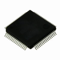
VSC8601XKN Vitesse Semiconductor Corp, VSC8601XKN Datasheet - Page 35

VSC8601XKN
Manufacturer Part Number
VSC8601XKN
Description
IC PHY 10/100/1000 64-EP-LQFP
Manufacturer
Vitesse Semiconductor Corp
Type
PHY Transceiverr
Specifications of VSC8601XKN
Number Of Drivers/receivers
1/1
Protocol
Gigabit Ethernet
Voltage - Supply
2.5V, 3.3V
Mounting Type
Surface Mount
Package / Case
64-LQFP Exposed Pad, 64-eLQFP, 64-HLQFP
Case
TQFP
Dc
06+
Lead Free Status / RoHS Status
Lead free / RoHS Compliant
Other names
907-1028
Available stocks
Company
Part Number
Manufacturer
Quantity
Price
Company:
Part Number:
VSC8601XKN
Manufacturer:
KYOCERA/AVX
Quantity:
20 000
Company:
Part Number:
VSC8601XKN
Manufacturer:
VITESSE
Quantity:
1 235
Company:
Part Number:
VSC8601XKN
Manufacturer:
Vitesse Semiconductor Corporation
Quantity:
10 000
Part Number:
VSC8601XKN
Manufacturer:
VITESSE
Quantity:
20 000
Table 4.
Table 5.
Revision 4.1
September 2009
SAMPLE/PRELOAD Allows a snapshot of inputs and outputs during normal system
operation to be taken and examined. It also allows data values to be loaded into the
boundary-scan cells prior to the selection of other boundary-scan test instructions.
IDCODE Provides the version number (bits 31:28), part number (bits 27:12), and the
manufacturer identity (bits 11:1) to be serially read from the device.
The following table provides information about the meaning of IDCODE binary values
stored in the device JTAG registers.
JTAG Device Identification Register Description
CLAMP Allows the state of the signals driven from the component pins to be
determined from the boundary-scan register while the bypass register is selected as the
serial path between TDI and TDO. While the CLAMP instruction is selected, the signals
driven from the component pins do not change.
HIGHZ Places the component in a state in which all of its system logic outputs are
placed in a high impedance state. In this state, an in-circuit test system may drive
signals onto the connections normally driven by a component output without incurring a
risk of damage to the component. This makes it possible to use a board where not all of
the components are compatible with the IEEE 1149.1 standard.
BYPASS The bypass register contains a single shift-register stage and is used to
provide a minimum-length serial path (one TCK clock period) between TDI and TDO to
bypass the device when no test operation is required.
The following table provides more information about the location and IEEE compliance
of the JTAG instruction codes used in the VSC8601.
JTAG Interface Instruction Codes
Description
Bit field
Binary value
Instruction
EXTEST
SAMPLE/PRELOAD
IDCODE
CLAMP
HIGHZ
BYPASS
RESERVED
Device Version
Number
31 through 28
0001
Code
0000
0001
0110
0010
0011
1111
0100, 0101,
0111, 1000-1110
Model Number
27 through 12
1000 0110 0000 0001 000 0111 0100
Selected Register
Boundary-scan
Boundary-scan
Device identification
Bypass register
Bypass register
Bypass register
Manufacturing
Identity
11 through 1
Register
Width
45
45
32
1
1
1
Functional Descriptions
VSC8601 Datasheet
IEEE 1149.1
Specification
Mandatory
Mandatory
Optional
Optional
Optional
Mandatory
Page 35
LSB
0
1


