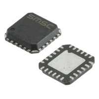
LAN8700IC-AEZG SMSC, LAN8700IC-AEZG Datasheet - Page 12

LAN8700IC-AEZG
Manufacturer Part Number
LAN8700IC-AEZG
Description
TXRX ETHERNET 10/100 IND 36-QFN
Manufacturer
SMSC
Type
Transceiverr
Datasheet
1.LAN8700C-AEZG.pdf
(80 pages)
Specifications of LAN8700IC-AEZG
Protocol
MII, RMII
Voltage - Supply
3 V ~ 3.6 V
Mounting Type
Surface Mount
Package / Case
36-QFN
Supply Voltage Range
3V To 3.6V
Digital Ic Case Style
QFN
No. Of Pins
36
Operating Temperature Range
-40°C To +85°C
Control Interface
MII, RMII
Data Rate Max
100Mbps
Rohs Compliant
Yes
Lead Free Status / RoHS Status
Lead free / RoHS Compliant
Number Of Drivers/receivers
-
Other names
638-1047-6
Available stocks
Company
Part Number
Manufacturer
Quantity
Price
Company:
Part Number:
LAN8700IC-AEZG
Manufacturer:
SANKEN
Quantity:
300
Company:
Part Number:
LAN8700IC-AEZG
Manufacturer:
Standard
Quantity:
34 317
Part Number:
LAN8700IC-AEZG
Manufacturer:
SMSC
Quantity:
20 000
Part Number:
LAN8700IC-AEZG-C3
Manufacturer:
SMSC
Quantity:
20 000
Part Number:
LAN8700IC-AEZG-TR
Manufacturer:
MICROCHIP/微芯
Quantity:
20 000
Chapter 3 Pin Description
Revision 2.2 (12-04-09)
3.1
SIGNAL NAME
I/O Signals
This chapter describes the signals on each pin. When a lower case “n” is used at the beginning of the
signal name, it indicates that the signal is active low. For example, nRST indicates that the reset signal
is active low.
The following buffer types are shown in the TYPE column of the tables in this chapter.
Note: The digital signals are not 5V tolerant.They are variable voltage from +1.6V to +3.6V.
TX_ER/
TX_EN
TXD0
TXD1
TXD2
TXD3
TXD4
nINT/
I
IPD
O
OPD
I/O
IOPD
IOPU
AI
AO
Input. Digital LVCMOS levels.
Input with internal pull-down. Digital LVCMOS levels.
Output. Digital LVCMOS levels.
Output with internal pull-down. Digital LVCMOS levels.
Input or Output . Digital LVCMOS levels.
Input or Output with internal pull-down. Digital LVCMOS levels.
Input or Output with internal pull-up. Digital LVCMOS levels.
Input. Analog levels..
Output. Analog levels.
TYPE
IOPU
±15kV ESD Protected MII/RMII 10/100 Ethernet Transceiver with HP Auto-MDIX Support and flexPWR
IPD
I
I
I
I
Table 3.1 MII Signals
DATASHEET
Transmit Data 0: Bit 0 of the 4 data bits that are accepted by
the PHY for transmission.
Transmit Data 1: Bit 1 of the 4 data bits that are accepted by
the PHY for transmission.
Transmit Data 2: Bit 2 of the 4 data bits that are accepted by
the PHY for transmission
Note:
Transmit Data 3: Bit 3 of the 4 data bits that are accepted by
the PHY for transmission.
Note:
MII Transmit Error: When driven high, the 4B/5B encode
process substitutes the Transmit Error code-group (/H/) for the
encoded data word. This input is ignored in 10Base-T operation.
MII Transmit Data 4: In Symbol Interface (5B Decoding) mode,
this signal becomes the MII Transmit Data 4 line, the MSB of the
5-bit symbol code-group.
Notes:
Transmit Enable: Indicates that valid data is presented on the
TXD[3:0] signals, for transmission. In RMII Mode, only TXD[1:0]
have valid data.
This signal is not used in RMII Mode.
This signal is mux’d with nINT
See
for additional information on configuration/strapping options.
Section 4.10, "nINT/TX_ER/TXD4 Strapping," on page 31
12
This signal should be grounded in RMII Mode.
This signal should be grounded in RMII Mode
DESCRIPTION
SMSC LAN8700/LAN8700i
®
Technology in a Small Footprint
Datasheet


