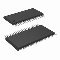
DS90CR217MTD/NOPB National Semiconductor, DS90CR217MTD/NOPB Datasheet

DS90CR217MTD/NOPB
Specifications of DS90CR217MTD/NOPB
*DS90CR217MTD/NOPB
DS90CR217MTD
Related parts for DS90CR217MTD/NOPB
DS90CR217MTD/NOPB Summary of contents
Page 1
... TTL interfaces. Block Diagram DS90CR217 Order Number DS90CR217MTD See NS Package Number MTD48 © 2006 National Semiconductor Corporation Features MHz shift clock support n 50% duty cycle on receiver output clock n Best-in-Class Set & Hold Times on TxINPUTs n Low power consumption ± ...
Page 2
Typical Application www.national.com 2 20190323 ...
Page 3
... Absolute Maximum Ratings If Military/Aerospace specified devices are required, please contact the National Semiconductor Sales Office/ Distributors for availability and specifications. Supply Voltage ( CMOS/TTL Input Voltage −0. CMOS/TTL Output Voltage −0. LVDS Receiver Input Voltage −0. LVDS Driver Output Voltage −0. LVDS Output Short ...
Page 4
Transmitter Switching Characteristics Over recommended operating supply and temperature ranges unless otherwise specified Symbol LLHT LVDS Low-to-High Transition Time (Figure 2) LHLT LVDS High-to-Low Transition Time (Figure 2) TCIT TxCLK IN Transition Time (Figure 3) TPPos0 Transmitter Output Pulse Position ...
Page 5
AC Timing Diagrams FIGURE 2. DS90CR217 (Transmitter) LVDS Output Load and Transition Times FIGURE 3. D590CR217 (Transmitter) Input Clock Transition Time FIGURE 1. “Worst Case” Test Pattern 20190303 5 20190302 20190304 20190307 www.national.com ...
Page 6
AC Timing Diagrams Note 5: Measurements DIFF Note 6: TCCS measured between earliest and latest LVDS edges Note 7: TxCLK Differential Low → High Edge FIGURE 4. DS90CR217 (Transmitter) Channel-to-Channel Skew FIGURE 5. DS90CR217 (Transmitter) Setup/Hold ...
Page 7
AC Timing Diagrams (Continued) FIGURE 7. DS90CR217 (Transmitter) Phase Lock Loop Set Time FIGURE 8. 21 Parallel TTL Data Inputs Mapped to LVDS Outputs (DS90CR217) FIGURE 9. Transmitter Powerdown Delay 7 20190313 20190316 20190317 www.national.com ...
Page 8
AC Timing Diagrams FIGURE 10. Transmitter LVDS Output Pulse Position Measurement Applications Information DS90CR217 Pin Descriptions — Channel Link Transmitter Pin Name I/O No. TxIN I 21 TTL level input. TxOUT Positive LVDS differential data output. TxOUT− O ...
Page 9
Applications Information and with the maximum data transfer of 1.785 Gbit/s. Addi- tional applications information can be found in the following National Interface Application Notes #### Topic AN-1041 Introduction to Channel Link AN-1108 Channel Link PCB and Interconnect ...
Page 10
Applications Information DECOUPLING CAPACITORS Bypassing capacitors are needed to reduce the impact of switching noise which could limit performance. For a conser- vative approach three parallel-connected decoupling capaci- tors (Multi-Layered Ceramic type in surface mount form fac- tor) between each ...
Page 11
Applications Information FIGURE 13. Single-Ended and Differential Waveforms (Continued) 11 20190326 www.national.com ...
Page 12
... BANNED SUBSTANCE COMPLIANCE National Semiconductor follows the provisions of the Product Stewardship Guide for Customers (CSP-9-111C2) and Banned Substances and Materials of Interest Specification (CSP-9-111S2) for regulatory environmental compliance. Details may be found at: www.national.com/quality/green. ...


