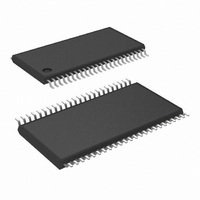
DS90CF364AMTD/NOPB National Semiconductor, DS90CF364AMTD/NOPB Datasheet - Page 10

DS90CF364AMTD/NOPB
Manufacturer Part Number
DS90CF364AMTD/NOPB
Description
IC RCVR LVDS FPD 18BIT 48-TSSOP
Manufacturer
National Semiconductor
Type
Driverr
Datasheets
1.DS90CF364AMTDNOPB.pdf
(14 pages)
2.DS90CF364MTD.pdf
(16 pages)
3.DS90CF364MTDNOPB.pdf
(16 pages)
Specifications of DS90CF364AMTD/NOPB
Number Of Drivers/receivers
1/0
Protocol
RS644
Voltage - Supply
3 V ~ 3.6 V
Mounting Type
Surface Mount
Package / Case
48-TSSOP
Number Of Drivers
21
Number Of Receivers
3
Data Rate
1300 Mbps
Operating Supply Voltage
3.3 V
Maximum Power Dissipation
1890 mW
Maximum Operating Temperature
+ 70 C
Minimum Operating Temperature
- 10 C
Mounting Style
SMD/SMT
Supply Voltage (max)
3.6 V
Supply Voltage (min)
3 V
Supply Current
60mA
Supply Voltage Range
3V To 3.6V
Driver Case Style
TSSOP
No. Of Pins
48
Operating Temperature Range
-10°C To +70°C
Msl
MSL 2 - 1 Year
Bandwidth
170GHz
Rohs Compliant
Yes
Lead Free Status / RoHS Status
Lead free / RoHS Compliant
Other names
*DS90CF364AMTD
*DS90CF364AMTD/NOPB
DS90CF364AMTD
*DS90CF364AMTD/NOPB
DS90CF364AMTD
Available stocks
Company
Part Number
Manufacturer
Quantity
Price
Company:
Part Number:
DS90CF364AMTD/NOPB
Manufacturer:
TI
Quantity:
106
www.national.com
RxIN+
RxIN−
RxOUT
RxCLK IN+
RxCLK IN−
RxCLK OUT
PWR DOWN
V
GND
PLL V
PLL GND
LVDS V
LVDS GND
CC
C—Setup and Hold Time (Internal data sampling window) defined by Rspos (receiver input strobe position) min and max
Tppos—Transmitter output pulse position (min and max)
RSKM = Cable Skew (type, length) + Source Clock Jitter (cycle to cycle) + ISI (Inter-symbol interference)
Cable Skew—typically 10 ps–40 ps per foot, media dependent
Note 9: Cycle-to-cycle jitter is less than 250 ps at 65 MHz.
Note 10: ISI is dependent on interconnect length; may be zero.
DS90CF384A Pin Descriptions — 56L TSSOP Package — 24-Bit FPD Link
Receiver
Pin Name
CC
CC
I/O No.
O
O
I
I
I
I
I
I
I
I
I
I
I
28
4
4
1
1
1
1
4
5
1
2
1
3
Positive LVDS differentiaI data inputs.
Negative LVDS differential data inputs.
TTL level data outputs. This includes: 8 Red, 8 Green, 8 Blue, and 3 control lines—FPLINE, FPFRAME,
DRDY (also referred to as HSYNC, VSYNC, Data Enable).
Positive LVDS differential clock input.
Negative LVDS differential clock input.
TTL Ievel clock output. The falling edge acts as data strobe.
TTL level input. When asserted (low input) the receiver outputs are low.
Power supply pins for TTL outputs.
Ground pins for TTL outputs.
Power supply for PLL.
Ground pin for PLL.
Power supply pin for LVDS inputs.
Ground pins for LVDS inputs.
FIGURE 13. Receiver LVDS Input Skew Margin
10
Description
10087011


