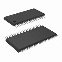
DS90CF364AMTD/NOPB National Semiconductor, DS90CF364AMTD/NOPB Datasheet

DS90CF364AMTD/NOPB
Specifications of DS90CF364AMTD/NOPB
*DS90CF364AMTD/NOPB
DS90CF364AMTD
Available stocks
Related parts for DS90CF364AMTD/NOPB
DS90CF364AMTD/NOPB Summary of contents
Page 1
... This chipset is an ideal means to solve EMI and cable size problems associated with wide, high speed TTL interfaces. Block Diagrams TRI-STATE ® registered trademark of National Semiconductor Corporation. © 1999 National Semiconductor Corporation DS012886 Features MHz shift clock support n Programmable Transmitter (DS90C363) strobe select (Rising or Falling edge strobe) n Single 3 ...
Page 2
Block Diagrams (Continued) www.national.com DS90C363 DS012886-1 Order Number DS90C363MTD See NS Package Number MTD48 DS90CF364 DS012886-24 Order Number DS90CF364MTD See NS Package Number MTD48 2 ...
Page 3
... Absolute Maximum Ratings If Military/Aerospace specified devices are required, please contact the National Semiconductor Sales Office/ Distributors for availability and specifications. Supply Voltage ( CMOS/TTL Input Voltage −0. CMOS/TTL Output Voltage −0. LVDS Receiver Input Voltage −0. LVDS Driver Output Voltage −0. LVDS Output Short Circuit ...
Page 4
Electrical Characteristics Over recommended operating supply and temperature ranges unless otherwise specified. Symbol Parameter TRANSMITTER SUPPLY CURRENT ICCTZ Transmitter Supply Current Power Down RECEIVER SUPPLY CURRENT ICCRW Receiver Supply Current, Worst Case ICCRG Receiver Supply Current, 16 Grayscale ICCRZ Receiver ...
Page 5
Transmitter Switching Characteristics Over recommended operating supply and −40˚C to +85˚C ranges unless otherwise specified Symbol Parameter LLHT LVDS Low-to-High Transition Time (Figure 3 ) LVDS High-to-Low Transition Time (Figure 3 ) LHLT TCIT TxCLK IN Transition Time (Figure 5 ...
Page 6
Receiver Switching Characteristics Over recommended operating supply and −40˚C to +85˚C ranges unless otherwise specified Symbol CLHT CMOS/TTL Low-to-High Transition Time (Figure 4 ) CMOS/TTL High-to-Low Transition Time (Figure 4 ) CHLT RSPos0 Receiver Input Strobe Position for Bit 0 ...
Page 7
AC Timing Diagrams (Continued) FIGURE 2. “16 Grayscale” Test Pattern (Notes Note 6: The worst case test pattern produces a maximum toggling of digital circuits, LVDS I/O and CMOS/TTL I/O. Note 7: The 16 grayscale test ...
Page 8
AC Timing Diagrams (Continued) Measurements at Vdiff=0V TCCS measured between earliest and latest LVDS edges TxCLK Differential Low High Edge FIGURE 6. DS90C363 (Transmitter) Channel-to-Channel Skew FIGURE 7. DS90C363 (Transmitter) Setup/Hold and High/Low Times FIGURE 8. DS90CF364 (Receiver) Setup/Hold and ...
Page 9
AC Timing Diagrams (Continued) FIGURE 10. DS90CF364 (Receiver) Clock In to Clock Out Delay FIGURE 11. DS90C363 (Transmitter) Phase Lock Loop Set Time FIGURE 12. DS90CF364 (Receiver) Phase Lock Loop Set Time DS012886-6 DS012886-20 DS012886-7 9 www.national.com ...
Page 10
AC Timing Diagrams (Continued) FIGURE 13. Seven Bits of LVDS in One Clock Cycle FIGURE 14. 21 Parallel TTL Data Inputs Mapped to LVDS Outputs www.national.com FIGURE 15. Transmitter Power Down Delay FIGURE 16. Receiver Power Down Delay 10 DS012886-9 ...
Page 11
AC Timing Diagrams (Continued) FIGURE 17. Transmitter LVDS Output Pulse Position Measurement 11 DS012886-22 www.national.com ...
Page 12
AC Timing Diagrams (Continued) FIGURE 18. Receiver LVDS Input Strobe Position www.national.com 12 DS012886-25 ...
Page 13
AC Timing Diagrams (Continued) C — Setup and Hold Time (Internal data sampling window) defined by Rspos (receiver input strobe position) min and max Tppos — Transmitter output pulse position (min and max) RSKM = Cable Skew (type, length) + ...
Page 14
DS90CF364 Pin Description — FPD Link Receiver Pin Name I/O No. RxIN Positive LVDS differentiaI data inputs. RxIN− Negative LVDS differential data inputs. RxOUT O 21 TTL level data outputs. This includes: 6 Red, 6 Green, ...
Page 15
Pin Diagram DS90C363 Pin R_FB R_FB DS90CF364 DS012886-23 TABLE 1. Programmable Transmitter Condition Strobe Status R_FB = V Rising edge strobe CC R_FB = GND Falling edge strobe 15 DS012886-13 www.national.com ...
Page 16
... NATIONAL’S PRODUCTS ARE NOT AUTHORIZED FOR USE AS CRITICAL COMPONENTS IN LIFE SUPPORT DEVICES OR SYSTEMS WITHOUT THE EXPRESS WRITTEN APPROVAL OF THE PRESIDENT AND GENERAL COUNSEL OF NATIONAL SEMICONDUCTOR CORPORATION. As used herein: 1. Life support devices or systems are devices or systems which, (a) are intended for surgical implant ...


