DS90CF364AMTD/NOPB National Semiconductor, DS90CF364AMTD/NOPB Datasheet - Page 5
DS90CF364AMTD/NOPB
Manufacturer Part Number
DS90CF364AMTD/NOPB
Description
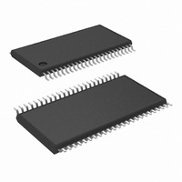
IC RCVR LVDS FPD 18BIT 48-TSSOP
Manufacturer
National Semiconductor
Type
Driverr
Datasheets
1.DS90CF364AMTDNOPB.pdf
(14 pages)
2.DS90CF364MTD.pdf
(16 pages)
3.DS90CF364MTDNOPB.pdf
(16 pages)
Specifications of DS90CF364AMTD/NOPB
Number Of Drivers/receivers
1/0
Protocol
RS644
Voltage - Supply
3 V ~ 3.6 V
Mounting Type
Surface Mount
Package / Case
48-TSSOP
Number Of Drivers
21
Number Of Receivers
3
Data Rate
1300 Mbps
Operating Supply Voltage
3.3 V
Maximum Power Dissipation
1890 mW
Maximum Operating Temperature
+ 70 C
Minimum Operating Temperature
- 10 C
Mounting Style
SMD/SMT
Supply Voltage (max)
3.6 V
Supply Voltage (min)
3 V
Supply Current
60mA
Supply Voltage Range
3V To 3.6V
Driver Case Style
TSSOP
No. Of Pins
48
Operating Temperature Range
-10°C To +70°C
Msl
MSL 2 - 1 Year
Bandwidth
170GHz
Rohs Compliant
Yes
Lead Free Status / RoHS Status
Lead free / RoHS Compliant
Other names
*DS90CF364AMTD
*DS90CF364AMTD/NOPB
DS90CF364AMTD
*DS90CF364AMTD/NOPB
DS90CF364AMTD
Available stocks
Company
Part Number
Manufacturer
Quantity
Price
Company:

Part Number:
DS90CF364AMTD/NOPB
Manufacturer:
TI
Quantity:
106


LLHT
LHLT
TCIT
TCCS
TPPos0
TPPos1
TPPos2
TPPos3
TPPos4
TPPos5
TPPos6
TCIP
TCIH
TCIL
TSTC
THTC
TCCD
TPLLS
TPDD
Symbol
Over recommended operating supply and −40˚C to +85˚C ranges unless otherwise specified
Transmitter Switching Characteristics
LVDS Low-to-High Transition Time (Figure 3 )
LVDS High-to-Low Transition Time (Figure 3 )
TxCLK IN Transition Time (Figure 5 )
TxOUT Channel-to-Channel Skew (Figure 6 )
Transmitter Output Pulse Position for Bit 0
(Figure 17 )
Transmitter Output Pulse Position for Bit 1
Transmitter Output Pulse Position for Bit 2
Transmitter Output Pulse Position for Bit 3
Transmitter Output Pulse Position for Bit 4
Transmitter Output Pulse Position for Bit 5
Transmitter Output Pulse Position for Bit 6
TxCLK IN Period (Figure 7)
TxCLK IN High Time (Figure 7)
TxCLK IN Low Time (Figure 7)
TxIN Setup to TxCLK IN (Figure 7 )
TxIN Hold to TxCLK IN (Figure 7 )
TxCLK IN to TxCLK OUT Delay 25˚C, V
Transmitter Phase Lock Loop Set (Figure 11 )
Transmitter Power Down Delay (Figure 15 )
Parameter
CC
= 3.3V (Figure 9 )
5
f = 65 MHz
f = 65 MHz
0.35T
0.35T
−0.4
10.6
12.8
Min
1.8
4.0
6.2
8.4
2.5
3.0
15
0
0.75
0.75
11.0
13.2
0.5T
0.5T
Typ
250
2.2
4.4
6.6
8.8
3.7
0
T
0.65T
0.65T
Max
11.3
13.5
100
1.5
1.5
0.3
2.5
4.7
6.9
9.1
5.5
50
10
5
www.national.com
Units
ms
ns
ns
ns
ps
ns
ns
ns
ns
ns
ns
ns
ns
ns
ns
ns
ns
ns
ns
Related parts for DS90CF364AMTD/NOPB
Image
Part Number
Description
Manufacturer
Datasheet
Request
R

Part Number:
Description:
National Semiconductor [8-Bit D/A Converter]
Manufacturer:
National Semiconductor
Datasheet:
Part Number:
Description:
National Semiconductor [Media Coprocessor]
Manufacturer:
National Semiconductor
Datasheet:
Part Number:
Description:
Digitally Controlled Tone and Volume Circuit with Stereo Audio Power Amplifier, Microphone Preamp Stage and National 3D Sound
Manufacturer:
National Semiconductor
Datasheet:
Part Number:
Description:
Digitally Controlled Tone and Volume Circuit with Stereo Audio Power Amplifier, Microphone Preamp Stage and National 3D Sound
Manufacturer:
National Semiconductor
Datasheet:
Part Number:
Description:
AC97 Rev 2 Codec with Sample Rate Conversion and National 3D Sound
Manufacturer:
National Semiconductor
Part Number:
Description:
Manufacturer:
National Semiconductor
Datasheet:
Part Number:
Description:
Manufacturer:
National Semiconductor
Datasheet:
Part Number:
Description:
General Purpose, Low Voltage, Low Power, Rail-to-Rail Output Operational Amplifiers
Manufacturer:
National Semiconductor
Datasheet:
Part Number:
Description:
8-bit 20 MSPS flash A/D converter.
Manufacturer:
National Semiconductor
Datasheet:
Part Number:
Description:
Low Noise Quad Operational Amplifier
Manufacturer:
National Semiconductor
Datasheet:
Part Number:
Description:
Quad Differential Line Receivers
Manufacturer:
National Semiconductor
Datasheet:
Part Number:
Description:
Quad High Speed Trapezoidal? Bus Transceiver
Manufacturer:
National Semiconductor
Datasheet:
Part Number:
Description:
Dual Line Receiver
Manufacturer:
National Semiconductor
Datasheet:
Part Number:
Description:
TTL to 10k ECL Level Translator with Latch
Manufacturer:
National Semiconductor
Datasheet: