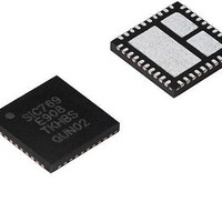
SIC779CD-T1-GE3 Vishay, SIC779CD-T1-GE3 Datasheet

SIC779CD-T1-GE3
Specifications of SIC779CD-T1-GE3
Related parts for SIC779CD-T1-GE3
SIC779CD-T1-GE3 Summary of contents
Page 1
... Halogen-free according to IEC 61249-2-21 definition • Compliant to RoHS Directive 2002/95/EC APPLICATIONS • CPU and GPU core voltage regulation • Server, computer, workstation, game console, graphics boards, PC BOOT V SWH PHASE SiC779CD Figure 1 This document is subject to change without notice. SiC779 Vishay Siliconix switching at 1 MHz ® MLP www ...
Page 2
... SiC779 Vishay Siliconix ORDERING INFORMATION Part Number SiC779CD-T1-GE3 SiC779DB ABSOLUTE MAXIMUM RATINGS (T Parameter Input Voltage Switch Node Voltage (DC) Drive Input Voltage Control Input Voltage Logic Pins Boot Voltage DC (referenced GND Boot Voltage < 200 ns Transient (referenced to C Boot to Phase Voltage DC Boot to Phase Voltage < 200 ns ...
Page 3
... VIN PWM d_on_HS r_HS f_HS PWM d_off_LS r_LS f_LS dead_on dead_off This document is subject to change without notice. SiC779 Vishay Siliconix Min. Typ. Max. 60 400 600 0.60 0.75 3.5 3.8 4.2 0.8 1.0 1.2 0.9 1.3 1.8 3.4 3.7 4.0 300 170 ...
Page 4
... SiC779 Vishay Siliconix TIMING DEFINITIONS Region Note referenced to the high side source referenced to the low side source SiC779 BLOCK DIAGRAM Thermal Monitor and Warning V CIN DSBL# V CIN PWM C Zero- GND Current Detect SMOD# www.vishay.com 4 THE PRODUCTS DESCRIBED HEREIN AND THIS DOCUMENT ARE SUBJECT TO SPECIFIC DISCLAIMERS, SET FORTH AT ...
Page 5
... UVLO falling edge triggers the shutdown of the device added precaution, a 20.2 k resistor is connected between GH and PHASE to provide a discharge path for the HS MOSFET. This document is subject to change without notice. SiC779 Vishay Siliconix ) IN and PHASE) SWH is the circuit PWM regulated output. ...
Page 6
... SiC779 Vishay Siliconix DEVICE TRUTH TABLE DSBL# SMOD Open TRISTATE PWM VOLTAGE THRESHOLD DIAGRAM PWM V th_pwm_r V th_tri_f V th_tri_r V th_pwm_f GH GL SMOD OPERATION DIAGRAM DSBL SMOD PWM www.vishay.com 6 THE PRODUCTS DESCRIBED HEREIN AND THIS DOCUMENT ARE SUBJECT TO SPECIFIC DISCLAIMERS, SET FORTH AT PWM ...
Page 7
... Figure 5 - PowerPAK MLP 40P Pin Out - Top View Description externally. All pins internally connected. GND This document is subject to change without notice. SiC779 Vishay Siliconix 30 V SWH 29 V SWH 28 P GND 27 P GND 26 P GND 25 P GND 24 P GND 23 P GND 22 P GND ...
Page 8
... SiC779 Vishay Siliconix ELECTRICAL CHARACTERISTICS 1.0 0.8 0.6 0.4 0.2 0 110 125 140 Temperature (°C) I (mA) vs. Temperature at Frequency = 300 kHz CIN CIN 1.3 1.2 1.1 1.0 0.9 0 110 125 140 Temperature (°C) PWM Falling Threshold (V) vs. Temperature (° CIN DRV 1.6 1 ...
Page 9
... DRV = 5 V 4.4 4.2 4.0 3.8 3.6 3.4 3.2 3 PWM Rising Tristate Threshold (V) vs. Temperature (°C) This document is subject to change without notice. SiC779 Vishay Siliconix 110 125 140 Temperature (° CIN DRV 110 125 140 Temperature (°C) (mA) vs. Temperature at Frequency = 1 MHz ...
Page 10
... SiC779 Vishay Siliconix ELECTRICAL CHARACTERISTICS 2.5 2.3 2.1 1.9 1.7 1.5 1.3 1.1 0.9 0.7 0.5 4.7 4.8 4.9 5.0 5.1 5.2 V (V) CIN DSBL Falling Threshold vs. V 2.5 2.3 2.1 1.9 1.7 1.5 1.3 1.1 0.9 0.7 0.5 4.7 4.8 4 ...
Page 11
... PWM: 2 V/div. GH: 5 V/div V/div. SWH V/div. SWH GL: 2 V/div. GL: 2 V/div. Switching Waveforms Load (PWM Falling Edge) = 500 kHz SW This document is subject to change without notice. SiC779 Vishay Siliconix V/div V/div. DRV CIN V : 0.5 V/div. OUT PWM: 3 V/div. Startup Ramping down ...
Page 12
... SiC779 Vishay Siliconix ELECTRICAL CHARACTERISTICS V/div. DRV CIN V/div. IN Time: 2 ms/div. Startup with V Ramping 1 OUT SW DSBL#: 2 V/div 0.5 V/div. OUT Time: 20 µs/div. Startup with DSBL# Toggle High 1 OUT V/div. IN PWM: 3 V/div 0.5 V/div. OUT Startup with PWM existing Tri-state 1 OUT SW www.vishay.com ...
Page 13
... SiC779 and inductor loss.) Figure MHz 10 8 500 kHz 6 4 300 kHz Load Current ( 1 Air Flow: IN OUT DRV CIN Inductance = 0.22 µH, DCR = 0.29 mΩ; (Power loss includes SiC779 and inductor loss.) Figure 6b This document is subject to change without notice. SiC779 Vishay Siliconix www.vishay.com www.vishay.com/doc?91000 13 ...
Page 14
... SiC779 Vishay Siliconix PACKAGE DIMENSIONS Pin 1 dot A by marking MLP66- mm) B Top View DIM Min. (8) 0. 0.00 A2 (4) 0. 0.35 (3) N (3) Nd (3) Ne D2-1 1.45 D2-2 1.45 D2-3 2.35 E2-1 4.35 E2-2 1.95 E2-3 1. Notes: 1. Use millimeters as the primary measurement. 2. Dimensioning and tolerances conform to ASME Y14.5M-1994. ...
Page 15
... Pocket position relative to sprocket hole measured as true position of pocket, not pocket hole. Vishay Siliconix maintains worldwide manufacturing capability. Products may be manufactured at one of several qualified locations. Reliability data for Silicon Technology and Package Reliability represent a composite of all qualified locations. For related documents such as package/tape drawings, part marking, and reliability data, see www ...
Page 16
... Vishay product could result in personal injury or death. Customers using or selling Vishay products not expressly indicated for use in such applications their own risk and agree to fully indemnify and hold Vishay and its distributors harmless from and against any and all claims, liabilities, expenses and damages arising or resulting in connection with such use or sale, including attorneys fees, even if such claim alleges that Vishay or its distributor was negligent regarding the design or manufacture of the part ...


