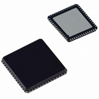
AD9958BCPZ Analog Devices Inc, AD9958BCPZ Datasheet - Page 21

AD9958BCPZ
Manufacturer Part Number
AD9958BCPZ
Description
IC DDS DUAL 500MSPS DAC 56LFCSP
Manufacturer
Analog Devices Inc
Datasheet
1.AD9958BCPZ.pdf
(44 pages)
Specifications of AD9958BCPZ
Design Resources
Low Jitter Sampling Clock Generator for High Performance ADCs Using AD9958/9858 and AD9515 (CN0109) Phase Coherent FSK Modulator (CN0186)
Resolution (bits)
10 b
Master Fclk
500MHz
Tuning Word Width (bits)
32 b
Voltage - Supply
1.71 V ~ 1.96 V
Operating Temperature
-40°C ~ 85°C
Mounting Type
Surface Mount
Package / Case
56-LFCSP
Pll Type
Frequency Synthesis
Frequency
500MHz
Supply Current
105mA
Supply Voltage Range
1.71V To 1.89V
Digital Ic Case Style
LFCSP
No. Of Pins
56
Operating Temperature Range
-40°C To +85°C
Lead Free Status / RoHS Status
Lead free / RoHS Compliant
For Use With
AD9958/PCBZ - BOARD EVALUATION FOR AD9958
Lead Free Status / Rohs Status
Compliant
Available stocks
Company
Part Number
Manufacturer
Quantity
Price
Company:
Part Number:
AD9958BCPZ
Manufacturer:
ADI
Quantity:
636
Part Number:
AD9958BCPZ
Manufacturer:
ADI/亚德诺
Quantity:
20 000
SCALABLE DAC REFERENCE CURRENT CONTROL
MODE
R
currents are equal by default. The scalable DAC reference can
be used to set the full-scale current of each DAC independent
from one another. This is accomplished by using the register
bits CFR[9:8]. Table 5 shows how each DAC can be individually
scaled for independent channel control. This scaling provides
for binary attenuation.
Table 5. DAC Full-Scale Current Control
CFR[9:8]
11
01
10
00
POWER-DOWN FUNCTIONS
The AD9958 supports an externally controlled power-down
feature and the more common software programmable power-
down bits found in previous Analog Devices DDS products.
The software control power-down allows the input clock circui-
try, the DAC, and the digital logic (for each separate channel) to
be individually powered down via unique control bits (CFR[7:6]).
These bits are not active when the externally controlled power-
down pin (PWR_DWN_CTL) is high. When the input pin,
PWR_DWN_CTL, is high, the AD9958 enters a power-down
mode based on the FR1[6] bit. When the PWR_DWN_CTL
input pin is low, the external power-down control is inactive.
When FR1[6] = 0 and the PWR_DWN_CTL input pin is high,
the AD9958 is put into a fast recovery power-down mode. In
this mode, the digital logic and the DAC digital logic are powered
down. The DAC bias circuitry, PLL, oscillator, and clock input
circuitry are not powered down.
SET
is common to all four DACs. As a result, the full-scale
25MHz
XTAL
Figure 35. Crystal Input Configuration
39pF
39pF
LSB Current State
Full scale
Half scale
Quarter scale
Eighth scale
REF_CLK
REF_CLK
PIN 23
PIN 22
Rev. A | Page 21 of 44
When FR1[6] = 1 and the PWR_DWN_CTL input pin is high,
the AD9958 is put into full power-down mode. In this mode, all
functions are powered down. This includes the DAC and PLL,
which take a significant amount of time to power up. When the
PLL is bypassed, the PLL is shut down to conserve power.
When the PWR_DWN_CTL input pin is high, the individual
power-down bits (CFR[7:6]) and (FR1[7]) are invalid (don’t
care) and unused. When the PWR_DWN_CTL input pin is low,
the individual power-down bits control the power-down modes
of operation.
Note that the power-down signals are all designed such that
Logic 1 indicates the low power mode and Logic 0 indicates the
powered-up mode.
MODULATION MODE
The AD9958 can perform 2-/4-/8-/16-level modulation of
frequency, phase, or amplitude. Modulation is achieved by
applying data to the profile pins. Each channel can be program-
med separately, but the ability to modulate multiple channels
simultaneously is constrained by the limited number of profile
pins. For instance, 16-level modulation uses all four profile pins,
which inhibits modulation for the remaining channel.
In addition, the AD9958 has the ability to ramp up or ramp
down the output amplitude before, during, or after a modulation
(FSK, PSK only) sequence. This is performed by using the 10-bit
output scalar. If the RU/RD feature is desired, unused profile
pins or unused SDIO_1/SDIO_2/SDIO_3 pins can be confi-
gured to initiate the operation. See the Output Amplitude
Control Mode section for more details of the RU/RD feature.
In modulation mode, each channel has its own set of control
bits to determine the type (frequency, phase, or amplitude)
of modulation. Each channel has 16 profile (channel word)
registers for flexibility. Register 0x0A through Register 0x18
are profile registers for modulation of frequency, phase, or
amplitude. Register 0x04, Register 0x05, and Register 0x06
are dedicated registers for frequency, phase, and amplitude,
respectively. These registers contain the first frequency, phase
offset, and amplitude word.
Frequency modulation has 32-bit resolution, phase modulation is
14 bits, and amplitude is 10 bits. When modulating phase or
amplitude, the word value must be MSB aligned in the profile
(channel word) registers and the unused bits are don’t care bits.
AD9958


