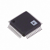
AD9953YSVZ Analog Devices Inc, AD9953YSVZ Datasheet - Page 25

AD9953YSVZ
Manufacturer Part Number
AD9953YSVZ
Description
IC DDS DAC 14BIT 400MSPS 48-TQFP
Manufacturer
Analog Devices Inc
Datasheet
1.AD9953YSVZ.pdf
(32 pages)
Specifications of AD9953YSVZ
Resolution (bits)
14 b
Master Fclk
400MHz
Tuning Word Width (bits)
32 b
Voltage - Supply
1.71 V ~ 1.96 V
Operating Temperature
-40°C ~ 105°C
Mounting Type
Surface Mount
Package / Case
48-TQFP Exposed Pad, 48-eTQFP, 48-HTQFP, 48-VQFP
Data Rate
25Mbps
Rf Ic Case Style
TQFP
No. Of Pins
48
Supply Voltage Range
1.71V To 1.89V, 3.135V To 3.465V
Operating Temperature Range
-40°C To +105°C
Msl
MSL 3 - 168 Hours
Frequency Max
400MHz
Lead Free Status / RoHS Status
Lead free / RoHS Compliant
For Use With
AD9953/PCB - BOARD EVAL FOR AD9953
Lead Free Status / RoHS Status
Lead free / RoHS Compliant, Lead free / RoHS Compliant
Available stocks
Company
Part Number
Manufacturer
Quantity
Price
Company:
Part Number:
AD9953YSVZ
Manufacturer:
Analog Devices Inc
Quantity:
135
Company:
Part Number:
AD9953YSVZ
Manufacturer:
ADI
Quantity:
329
Company:
Part Number:
AD9953YSVZ
Manufacturer:
Analog Devices Inc
Quantity:
10 000
Company:
Part Number:
AD9953YSVZ-REEL7
Manufacturer:
Analog Devices Inc
Quantity:
10 000
Synchronizing Multiple AD9953s
The AD9953 allows easy synchronization of multiple AD9953s.
There are three modes of synchronization available to the u
an automatic synchronization mode, a software controlled
manual synchronization mode, and a hardware controlled
manual synchronization mode. In all cases, when a user wants
to synchronize two or more devices, the following considera-
ti
clock source. Trace lengths and path impedance of the clock
tree must be designed to keep the phase delay of the different
clock branches as closely matched as possible. Second, the I/O
UPDATE signal’s rising edge must be provided synchronously
to all devices in the system. Finally, regardless of the internal
synchronization method used, the DVDD_I/O supply should
be set to 3.3 V for all devices that are to be synchronized.
AVDD and DVDD should be left at 1.8 V.
In automatic synchronization mode, one device is chosen as a
master; the other device(s) will be slaved to this master. When
configured in this mode, the slaves will automatically synchron-
ize their internal clocks to the SYNC_CLK output signal of the
master device. To enter automatic synchronization mode, set
the slave device’s automatic synchronization bit (CFR1<23> =
1). Connect the SYNC_IN input(s) to the master SYNC_CLK
output. The slave device will continuously update the phase
relationship of its SYNC_CLK until it is in phase with the
SYNC_IN input, which is the SYNC_CLK of the master device.
When attempting to synchronize devices running at SYSCLK
speeds beyond 250 MSPS, the high speed sync enhancement
enable bit should be set (CFR2<11> = 1).
I
d
c
sy
s
cl
m
n software manual synchronization mode, the user forces the
ynchronization bit (CFR1<22> = 1). The bit (CFR1<22>) will be
ycle (1/4 SYNC_CLK period). To activate the manual
evice to advance the SYNC_CLK rising edge one SYSCLK
ons must be observed. First, all units must share a common
eared immediately. To advance the rising edge of the SYNC_CLK
ultiple times, this bit will need to be set multiple times.
nchronization mode, set the slave device’s software manual
I/O BUFFERS
REGISTERS
I/O UPDATE
SYNC_CLK
SYSCLK
DATA IN
DATA IN
DATA 1
THE DEVICE REGISTERS AN I/O UPDATE AT POINT A.
DATA 0
A
B
Figure
DA
22. I/O Synchronization Tim
TA 2
ser:
Rev. A | Page 25 of 32
THE DATA IS TRANS
In h
inpu
e
ri
w
synchronization bit (CFR2<10> = 1). Unlike the software
manual synchronization bit, this bit does not self clear. Once the
hardware manual synchronization mode is enabled, all rising
edges detected on the SYNC_IN input will cause the device to
advance the rising edge of the SYNC_CLK by one SYSCLK
cycle until this enable bit is cleared (CFR2<10> = 0).
Using a Single Crystal to Drive Multiple AD9953 Clock
Inputs
The AD9953 crystal oscillator output signal is available on the
CRYSTAL OUT pin, enabling one crystal to drive multiple
AD9953s. In order to drive multiple AD9953s with one crystal,
the CRYSTAL OUT pin of the AD9953 using the external crystal
should be connected to the REFCLK input of the other AD9953.
The CRYSTAL OUT pin is static until the CFR2<9> bit is set,
enabling the output. The drive strength of the CRYSTAL OUT
pin is typically very low, so this signal should be buffered prior
to using it to drive any loads.
SERIAL PORT OPERATION
With the AD9953, the instruction byte specifies read/write
operation and the register address. Serial operations on the
AD9953 occur only at the register level, not the byte level. For
the AD9953, th
tion byte register address and automatically generates the
proper register byte address. In addition, the controller expects
that all bytes of that register will be accessed. It is required that
all bytes of a register be accessed during serial I/O operations,
with one exception. The IOSYNC function can be used to abort
an I/O operation, thereby allowing some, but not all bytes to be
accessed.
DATA
dge of the SYNC_CLK signal each time the device detects a
sing edge on the SYNC_IN pin. To put the device into hard-
are manual synchronization mode, set the hardware manual
ardware manual synchronization mode, the SYNC_IN
FERRED FROM THE I/O BUFFERS AT POINT B.
ing Diagram
t pin is
1
configured such that it will now advance the rising
e serial po t controller recognizes the instruc-
A
r
DATA 3
B
DATA 2
AD9953


