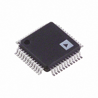
AD9953YSVZ Analog Devices Inc, AD9953YSVZ Datasheet - Page 23

AD9953YSVZ
Manufacturer Part Number
AD9953YSVZ
Description
IC DDS DAC 14BIT 400MSPS 48-TQFP
Manufacturer
Analog Devices Inc
Datasheet
1.AD9953YSVZ.pdf
(32 pages)
Specifications of AD9953YSVZ
Resolution (bits)
14 b
Master Fclk
400MHz
Tuning Word Width (bits)
32 b
Voltage - Supply
1.71 V ~ 1.96 V
Operating Temperature
-40°C ~ 105°C
Mounting Type
Surface Mount
Package / Case
48-TQFP Exposed Pad, 48-eTQFP, 48-HTQFP, 48-VQFP
Data Rate
25Mbps
Rf Ic Case Style
TQFP
No. Of Pins
48
Supply Voltage Range
1.71V To 1.89V, 3.135V To 3.465V
Operating Temperature Range
-40°C To +105°C
Msl
MSL 3 - 168 Hours
Frequency Max
400MHz
Lead Free Status / RoHS Status
Lead free / RoHS Compliant
For Use With
AD9953/PCB - BOARD EVAL FOR AD9953
Lead Free Status / RoHS Status
Lead free / RoHS Compliant, Lead free / RoHS Compliant
Available stocks
Company
Part Number
Manufacturer
Quantity
Price
Company:
Part Number:
AD9953YSVZ
Manufacturer:
Analog Devices Inc
Quantity:
135
Company:
Part Number:
AD9953YSVZ
Manufacturer:
ADI
Quantity:
329
Company:
Part Number:
AD9953YSVZ
Manufacturer:
Analog Devices Inc
Quantity:
10 000
Company:
Part Number:
AD9953YSVZ-REEL7
Manufacturer:
Analog Devices Inc
Quantity:
10 000
OSK Ramp Rate Timer
The OSK ramp rate timer is a loadable down counter, which
generates the clock signal to the 14-bit counter that generates
the internal scale factor. The ramp rate timer is loaded with the
value of the ASFR every time the counter reaches 1 (decimal).
This load and countdown operation continues for as long as the
timer is enabled, unless the timer is forced to load before
reaching a count of 1.
If the load OSK timer bit (CFR1<26>) is set, the ramp rate
timer is loaded upon an I/O UPDATE or upon reaching a value
of 1. The ramp timer can be loaded before reaching
by three methods.
DDS CORE
AMPLITUDE SCALE
FACTOR REGISTER
COS(X)
(ASF)
0
1
Figure 20. On-Of
0
a cou
OSK ENAB
nt of 1
FA
CFR<25
OUT
OSK PIN
Rev. A | Page 23 of 32
INC/D
CTOR GENERATO
AUTO SCALE
f Shaped Key
LE
>
EC ENABLE
UP/DN
HOLD
TO D
SYN
C_CLK
AC
ing Block Diagram
T
W
lo
d
T
lo
(C
T
l
in
sh
b
oaded before reaching a count of 1 is when going from the
R
own as normal.
eing set.
he first method of loading is by changing the OSK input pin.
he second method in which the sweep ramp rate timer can be
he third method in which the sweep ramp rate timer can be
aded into the ramp rate timer, which then proceeds to count
aded before reaching a count of 1 is if the load OSK timer bit
active auto shaped on-off keying mode to the active auto
aped on-off keying mode; that is, when the sweep enable bit is
hen the OSK input pin changes state, the ASFR value is
FR1<26>) is set and an I/O UPDATE is issued.
AUTO DESK
CFR1<24>
ENABLE
RAMP RATE TIMER
LOAD OSK TIMER
CFR1<26>
AMPLITUDE RAMP
RATE REGISTER
LOAD
(ASF)
DATA
EN
CLOCK
AD9953


