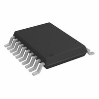
AD5930YRUZ Analog Devices Inc, AD5930YRUZ Datasheet - Page 23

AD5930YRUZ
Manufacturer Part Number
AD5930YRUZ
Description
IC GEN PROG FREQ BURST 20TSSOP
Manufacturer
Analog Devices Inc
Datasheet
1.AD5930YRUZ.pdf
(28 pages)
Specifications of AD5930YRUZ
Resolution (bits)
10 b
Master Fclk
50MHz
Tuning Word Width (bits)
24 b
Voltage - Supply
2.3 V ~ 5.5 V
Operating Temperature
-40°C ~ 125°C
Mounting Type
Surface Mount
Package / Case
20-TSSOP
Synthesizer Type
Frequency
Frequency
25MHz
Supply Voltage Range
2.3V To 5.5V
Supply Current
2.4mA
Operating Temperature Range
-40°C To +105°C
Digital Ic Case Style
TSSOP
No. Of Pins
20
Pin Count
20
Screening Level
Automotive
Package Type
TSSOP
Lead Free Status / RoHS Status
Lead free / RoHS Compliant
Lead Free Status / RoHS Status
Lead free / RoHS Compliant, Lead free / RoHS Compliant
Available stocks
Company
Part Number
Manufacturer
Quantity
Price
Company:
Part Number:
AD5930YRUZ
Manufacturer:
Intel
Quantity:
33
AD5930 TO 68HC11/68L11 INTERFACE
Figure 37 shows the serial interface between the AD5930 and
the 68HC11/68L11 µcontroller. The µcontroller is configured as
the master by setting bit MSTR in the SPCR to 1, which
provides a serial clock on SCK while the MOSI output drives
the serial data line SDATA. Since the µcontroller does not have
a dedicated frame sync pin, the FSYNC signal is derived from a
port line (PC7). The setup conditions for correct operation of
the interface are as follows:
1.
2.
When data is being transmitted to the AD5930, the FSYNC line
is taken low (PC7). Serial data from the 68HC11/68L11 is
transmitted in 8-bit bytes with only eight falling clock edges
occurring in the transmit cycle. Data is transmitted MSB first.
In order to load data into the AD5930, PC7 is held low after the
first 8 bits are transferred and a second serial write operation is
performed to the AD5930. Only after the second 8 bits have
been transferred should FSYNC be taken high again.
AD5930 TO 80C51/80L51 INTERFACE
Figure 38 shows the serial interface between the AD5930 and
the 80C51/80L51 µcontroller. The µcontroller is operated in
mode 0 so that TXD of the 80C51/80L51 drives SCLK of the
AD5930, while RXD drives the serial data line SDATA. The
FSYNC signal is again derived from a bit programmable pin on
the port (P3.3 being used in the diagram). When data is to be
transmitted to the AD5930, P3.3 is taken low. The 80C51/80L51
transmits data in 8-bit bytes, thus, only eight falling SCLK edges
occur in each cycle. To load the remaining 8 bits to the AD5930,
P3.3 is held low after the first 8 bits have been transmitted, and
SCK idles high between write operations (CPOL = 0)
Data is valid on the SCK falling edge (CPHA = 1)
1
ADDITIONAL PINS OMITTED FOR CLARITY.
68HC11/68L11
Figure 37. 68HC11/68L11 to AD5930 Interface
MOSI
SCK
PC7
1
FSYNC
SDATA
SCLK
AD5930
1
Rev. 0 | Page 23 of 28
a second write operation is initiated to transmit the second byte
of data. P3.3 is taken high following the completion of the
second write operation. SCLK should idle high between the two
write operations. The 80C51/80L51 outputs the serial data in an
LSB first format. The AD5930 accepts the MSB first (the 4
MSBs being the control information, the next 4 bits being the
address while the 8 LSBs contain the data when writing to a
destination register). Therefore, the transmit routine of the
80C51/80L51 must take this into account and rearrange the bits
so that the MSB is output first.
AD5930 TO DSP56002 INTERFACE
Figure 39 shows the interface between the AD5930 and the
DSP56002. The DSP56002 is configured for normal mode,
asynchronous operation with a gated internal clock (SYN = 0,
GCK = 1, SCKD = 1). The frame sync pin is generated internally
(SC2 = 1), the transfers are 16 bits wide (WL1 = 1, WL0 = 0), and
the frame sync signal frames the 16 bits (FSL = 0). The frame
sync signal is available on Pin SC2, but needs to be inverted
before being applied to the AD5930. The interface to the
DSP56000/DSP56001 is similar to that of the DSP56002.
1
1
ADDITIONAL PINS OMITTED FOR CLARITY.
ADDITIONAL PINS OMITTED FOR CLARITY.
80C51/80L51
DSP56002
Figure 38. 80C51/80L51 to AD5930 Interface
Figure 39. DSP56002 to AD5930 Interface
RXD
SCK
P3.3
TXD
STD
SC2
1
1
FSYNC
SDATA
SCLK
FSYNC
SDATA
SCLK
AD5930
AD5930
1
1
AD5930


