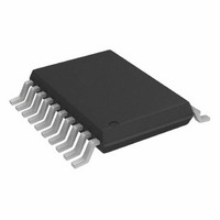
AD5930YRUZ Analog Devices Inc, AD5930YRUZ Datasheet - Page 18

AD5930YRUZ
Manufacturer Part Number
AD5930YRUZ
Description
IC GEN PROG FREQ BURST 20TSSOP
Manufacturer
Analog Devices Inc
Datasheet
1.AD5930YRUZ.pdf
(28 pages)
Specifications of AD5930YRUZ
Resolution (bits)
10 b
Master Fclk
50MHz
Tuning Word Width (bits)
24 b
Voltage - Supply
2.3 V ~ 5.5 V
Operating Temperature
-40°C ~ 125°C
Mounting Type
Surface Mount
Package / Case
20-TSSOP
Synthesizer Type
Frequency
Frequency
25MHz
Supply Voltage Range
2.3V To 5.5V
Supply Current
2.4mA
Operating Temperature Range
-40°C To +105°C
Digital Ic Case Style
TSSOP
No. Of Pins
20
Pin Count
20
Screening Level
Automotive
Package Type
TSSOP
Lead Free Status / RoHS Status
Lead free / RoHS Compliant
Lead Free Status / RoHS Status
Lead free / RoHS Compliant, Lead free / RoHS Compliant
Available stocks
Company
Part Number
Manufacturer
Quantity
Price
Company:
Part Number:
AD5930YRUZ
Manufacturer:
Intel
Quantity:
33
AD5930
Table 7. Description of Bits in the Control Register
Bit
D15
to
D12
D11
D10
D9
D8
D7
D6
D5
D4
D3
D2
D1
D0
Name
ADDR
B24
DAC ENABLE
SINE/TRI
MSBOUTEN
CW/BURST
INT/EXT
BURST
INT/EXT
INCR
MODE
SYNCSEL
SYNCOUTEN
Reserved
Reserved
Function
Register address bits.
Two write operations are required to load a complete word into the F
When B24 = 1, a complete word is loaded into a frequency register in two consecutive writes. The first write
contains the 12 LSBs of the frequency word and the next write contains the 12 MSBs. Refer to Table 5 for the
appropriate addresses. The write to the destination register occurs after both words have been loaded, so the
register never holds an intermediate value.
When B24 = 0, the 24-bit F
other containing the 12 LSBs. This means that the 12 MSBs of the frequency word can be altered independent of
the 12 LSBs and vice versa. This is useful if the complete 24-bit update is not required. To alter the 12 MSBs or the
12 LSBs, a single write is made to the appropriate register address. Refer to Table 5 for the appropriate addresses.
When DAC ENABLE = 1, the DAC is enabled.
When DAC ENABLE = 0, the DAC is powered down. This saves power and is beneficial when only using the MSB of
the DAC input data (available at the MSBOUT pin).
The function of this bit is to control what is available at the IOUT/IOUTB pins.
When SINE/TRI = 1, the SIN ROM is used to convert the phase information into amplitude information resulting in a
sinusoidal signal at the output.
When SINE/TRI = 0, the SIN ROM is bypassed, resulting in a triangular (up-down) output from the DAC.
When MSBOUTEN = 1, the MSBOUT pin is enabled.
When MSBOUTEN = 0, the MSBOUT is disabled (tri-state).
When CW/BURST = 1, the AD5930 outputs each frequency continuously for the length of time or number of output
waveform cycles specified in the appropriate register, T
When CW/BURST = 0, the AD5930 bursts each frequency for the length of time/number of cycles specified in the
burst register, T
outputs a DC value of midscale. In external increment mode, it is defined by the pulse widths on the CTRL pin.
This bit is active when D7 = 0 and is also used in conjunction with D5. When the user is incrementing the frequency
externally (D5 = 1), D6 dictates whether the user is controlling the burst internally or externally.
When INT/EXT BURST = 1, the output burst is controlled externally through the CTRL pin. This is useful if the user is
using an external source to both trigger the frequency increments and determine the burst interval.
When INT/EXT BURST = 0, the output burst is controlled internally. The burst is pre-programmed by the user into
the T
When D5 = 0, this bit is ignored.
When INT/EXT INCR = 1, the frequency increments are triggered externally through the CTRL pin.
When INT/EXT INCR = 0, the frequency increments are triggered automatically.
The function of this bit is to control what type of frequency sweep is carried out.
When MODE = 1, the frequency profile is a saw sweep.
When MODE = 0, the frequency profile is a triangular (up-down) sweep.
This bit is active when D2 = 1. It is user-selectable to pulse at the end of sweep (EOS) or at each frequency
increment.
When SYNCSEL = 1, the SYNCOP pin outputs a high level at the end of the sweep and returns to zero at the start of
the subsequent sweep.
When SYNCSEL= 0, the SYNCOP outputs a pulse of 4 × T
When SYNCOUTEN= 1, the SYNC output is available at the SYNCOP pin.
When SYNCOUTEN= 0, the SYNCOP pin is disabled (tri-state).
This bit must always be set to 1.
This bit must always be set to 1.
BURST
register (the burst interval can either be clock-based or for a specified number of output cycles).
BURST
. For the remainder of the time within each increment window (T
START
/∆f register operates as two 12-bit registers, one containing the 12 MSBs and the
Rev. 0 | Page 18 of 28
BURST
CLOCK
.
only at each frequency increment.
START
register and the ∆f register.
BURST
− t
INT
), the AD5930


