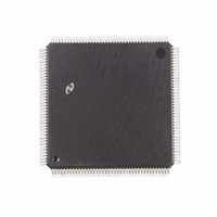
DP83934CVUL-33 National Semiconductor, DP83934CVUL-33 Datasheet - Page 61

DP83934CVUL-33
Manufacturer Part Number
DP83934CVUL-33
Description
IC CTRLR ORIENT NETWORK 160PQFP
Manufacturer
National Semiconductor
Datasheet
1.DP83934AVQB.pdf
(104 pages)
Specifications of DP83934CVUL-33
Controller Type
Network Interface Controller (NIC)
Interface
Twisted Pair
Voltage - Supply
4.75 V ~ 5.25 V
Current - Supply
140mA
Operating Temperature
0°C ~ 70°C
Mounting Type
Surface Mount
Package / Case
160-MQFP, 160-PQFP
Lead Free Status / RoHS Status
Contains lead / RoHS non-compliant
Other names
*DP83934CVUL-33
Available stocks
Company
Part Number
Manufacturer
Quantity
Price
Company:
Part Number:
DP83934CVUL-33
Manufacturer:
Texas Instruments
Quantity:
10 000
7 0 Bus Interface
7 3 5 3 Memory Cycle for BMODE
Asynchronous Mode
On the rising edge of T1 the SONIC-T asserts ECS to indi-
cate that the memory cycle is starting The address (A31–
A1) bus status (S2–S0) and the direction strobe (MRW) are
driven and do not change for the remainder of the memory
cycle On the falling edge of T1 the SONIC-T deasserts
ECS and asserts AS
In asynchronous mode DSACK0 1 are asynchronously
sampled on the falling edge of both T1 and T2 DSACK0 1
do not need to be synchronized to the bus clock because
the chip always resolves these signals to either a high or
low state If a synchronous termination of the bus cycle is
required however STERM may be used STERM is sam-
pled on the rising edge of T2 and must meet the setup and
hold times with respect to that edge for proper operation
Meeting the setup time for DSACK0 1 or STERM guaran-
tees that the SONIC-T will terminate the memory cycle 1 5
FIGURE 7-7 Memory Write BMODE
(Continued)
e
1
61
e
bus clocks after DSACK0 1 were sampled or 1 cycle after
STERM was sampled T2 states will be repeated until
DSACK0 1 or STERM are sampled properly in a low state
(see note below)
During read cycles ( Figures 7-8 and 7-9 ) data (D31– D0) is
latched at the falling edge of T2 and DS is asserted at the
falling edge of T1 For write cycles ( Figures 7-10 and 7-11 )
data is driven on the falling edge of T1 If there are wait
states inserted DS is asserted on the falling edge of the first
T2 (wait) DS is not asserted for zero wait state write cycles
The SONIC-T terminates the memory cycle by deasserting
AS and DS at the falling edge of T2
Note If the setup time for DSACK0 1 is met during T1 or the setup time for
1 Synchronous (1 Wait-State)
STERM is met during the first T2 the full asynchronous bus cycle will
take only 2 bus clocks This may be an unwanted situation If so
DSACK0 1 and STERM should normally be deasserted during T1 and
the start of T2 respectively
TL F 11719 – 34


