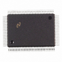
DP83902AVLJ National Semiconductor, DP83902AVLJ Datasheet - Page 9

DP83902AVLJ
Manufacturer Part Number
DP83902AVLJ
Description
IC CTRLR SER NETWORK IN 100PQFP
Manufacturer
National Semiconductor
Datasheet
1.DP83902AVJGNOPB.pdf
(70 pages)
Specifications of DP83902AVLJ
Controller Type
Serial Network Interface Controller
Interface
Serial
Voltage - Supply
4.75 V ~ 5.25 V
Current - Supply
140mA
Operating Temperature
0°C ~ 70°C
Mounting Type
Surface Mount
Package / Case
100-MQFP, 100-PQFP
Lead Free Status / RoHS Status
Contains lead / RoHS non-compliant
Other names
*DP83902AVLJ
Available stocks
Company
Part Number
Manufacturer
Quantity
Price
Company:
Part Number:
DP83902AVLJ
Manufacturer:
NS
Quantity:
2 500
Company:
Part Number:
DP83902AVLJ
Manufacturer:
RAYCHEM
Quantity:
2 500
Company:
Part Number:
DP83902AVLJ
Manufacturer:
Texas Instruments
Quantity:
10 000
Part Number:
DP83902AVLJ
Manufacturer:
NS/国半
Quantity:
20 000
4 0 Functional Description
TWISTED PAIR INTERFACE (TPI) MODULE
The TPI consists of five main logical functions
a) The Smart Squelch responsible for determining when
b) The Collision function checks for simultaneous transmis-
c) The Link Detector Generator checks the integrity of the
d) The Jabber disables the transmitter if it attempts to trans-
e) The Tx Driver
SMART SQUELCH
The ST-NIC implements an intelligent receive squelch on
the RXI
the receive inputs will not be mistaken for a valid signal
The squelch circuitry employs a combination of amplitude
and timing measurements to determine the validity of data
on the twisted pair inputs There are two squelch levels
which are selectable via the SQSEL pin One mode is
10BASE-T compatible and the second is reduced squelch
mode
The diagram shows the 10BASE-T mode operation of the
smart squelch
The signal at the start of packet is checked by the smart
squelch and any pulses not exceeding the squelch level
(either positive or negative depending upon polarity) will be
rejected Once this first squelch level is overcome correctly
the opposite squelch level must then be exceeded within
150 ns Finally the signal must exceed the original squelch
level within a further 150 ns to ensure that the input wave-
form will not be rejected The checking procedure results in
the loss of typically three bits at the beginning of each pack-
et
Only after all these conditions have been satisfied will a
control signal be generated to indicate to the remainder of
the circuitry that valid data is present At this time the smart
squelch circuitry is reset
Valid data is considered to be present until either squelch
level has not been generated for a time longer than 150 ns
indicating End of Packet Once good data has been detect-
ed the squelch levels are reduced to minimize the effect of
noise causing premature End of Packet detection
cable connecting the two twisted pair MAUs
valid data is present on the differential receive inputs
(RXI
sion and reception of data on the TXO
mit a longer than legal packet
coded data to the twisted pair network via the summing
resistors and transformer filter
g
g
)
differential inputs to ensure that impulse noise on
Pre-emphasis transmits Manchester en-
g
and RXI
(Refer to Figure 1 )
g
pins
9
The reduced squelch mode functions the same as the
10BASE-T mode except that only the lower level is used for
both turn-on and turn-off
COLLISION
A collision is detected by the TPI module when the receive
and transmit channels are active simultaneously If the TPI
is receiving when a collision is detected it is reported to the
controller immediately If however the TPI is transmitting
when a collision is detected the collision is not reported until
seven bits have been received while in the collision state
This prevents a collision being reported incorrectly due to
noise on the network The signal to the controller remains
for the duration of the collision
Approximately 1 s after the transmission of each packet a
signal called the Signal Quality Error (SQE) consisting of
typically 10 cycles of 10 MHz is generated This 10 MHz
signal also called the Heartbeat ensures the continued
functioning of the collision circuitry
LINK DETECTOR GENERATOR
The link generator is a timer circuit that generates a link
pulse as defined by the 10BASE-T specification that will be
generated by the transmitter section The pulse which is
100 ns wide is transmitted on the TXO
16 ms in the absence of transmit data
The pulse is used to check the integrity of the connection to
the remote MAU The link detection circuit checks for valid
pulses from the remote MAU and if valid link pulses are not
received the link detector will disable the transmit receive
and collision detection functions
The GDLNK output can directly drive a LED to show that
there is a good twisted pair link For normal conditions the
LED will be on The link integrity function can be disabled as
described in the Pin Description Section
JABBER
The jabber timer monitors the transmitter and disables the
transmission if the transmitter is active for greater than
26 ms The transmitter is then disabled for the whole time
that the ENDEC module’s internal transmit enable is assert-
ed This signal has to be deasserted for approximately
750 ms (the unjab time) before the Jabber re-enables the
transmit outputs
TRANSMIT DRIVER
The transmitter consists of four signals the true and com-
plement Manchester encoded data (TXO
nals delayed by 50 ns (TXOd
g
)
TL F 11157 – 5
g
a
) and these sig-
output every


