DP83902AVLJ National Semiconductor, DP83902AVLJ Datasheet
DP83902AVLJ
Specifications of DP83902AVLJ
Available stocks


Related parts for DP83902AVLJ


DP83902AVLJ Summary of contents
Page 1
... The ENDEC module interfaces directly to the transceiver module and also provides a fully IEEE compliant AUI (At- tachment Unit Interface) for connection to other media transceivers 1 0 System Diagram TRI-STATE is a registered trademark of National Semiconductor Corporation ST-NIC trademark of National Semiconductor Corporation C 1995 National Semiconductor Corporation ...
Page 2
General Description (Continued) The Media Access Control function which is provided by the Network Interface Control module (NIC) provides simple and efficient packet transmission and reception control by means of unique dual DMA channels and an internal FIFO Bus arbitration ...
Page 3
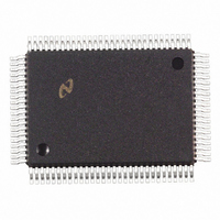
... Connection Diagrams (Continued) Order Number DP83902AVLJ See NS Package Number VLJ100A 11157 – 56 ...
Page 4
Connection Diagrams (Continued Pin Description PQFP PLCC AVJG Pin Pin No Pin No Pin No Name BUS INTERFACE PINS INT WACK PRD 99 100 8–11 96 RA3–RA0 1 2 ...
Page 5
Pin Description (Continued) PQFP PLCC AVJG Pin Pin No Pin No Pin No Name BUS INTERFACE PINS (Continued) 4 –8 12–23 2–4 6 AD0– 10 –12 28–31 7 9–15 AD15 20– ...
Page 6
Pin Description (Continued) PQFP PLCC AVJG Pin Pin No Pin No Pin No Name BUS INTERFACE PINS (Continued BACK BREQ RESET NETWORK INTERFACE PINS POL 49 ...
Page 7
Pin Description (Continued) PQFP PLCC AVJG Pin No Pin No Pin No NETWORK INTERFACE PINS (Continued ...
Page 8
Block Diagram Typical Connection to Twisted Pair Cable Recommended integrated modules are 1) Pulse Engineering PE65431 2) Belfuse 0556-2006-01 or 0556-3392-00 3) Valor FL1012 FIGURE 1 ST-NIC Twisted Pair Interface 11157 – ...
Page 9
Functional Description TWISTED PAIR INTERFACE (TPI) MODULE The TPI consists of five main logical functions a) The Smart Squelch responsible for determining when valid data is present on the differential receive inputs (RXI ) g b) The Collision ...
Page 10
Functional Description These four signals are resistively combined TXO TXOd and TXO with TXOd This is known as digital pre-emphasis and is required to compensate for the twisted pair cable which acts like a low ...
Page 11
Functional Description In order to prevent distortion on the transmitted frequency the total capacitance seen by the crystal should equal the total load capacitance On a standard parallel set-up as shown in the diagram below the 2 load ...
Page 12
Functional Description 3 ST-NIC flushes remaining bytes from FIFO 4 ST-NIC performs internal processing to prepare for writ- ing the header 5 ST-NIC writes 4-byte (2-word) header 6 ST-NIC de-asserts BREQ FIFO Threshold Detection To assure that no ...
Page 13
Transmit Receive Packet Encapsulation Decapsulation (Continued) SOURCE ADDRESS The source address is the physical address of the node that sent the packet Source addresses cannot be multicast or broadcast addresses This field is simply passed to buffer memory ...
Page 14
Packet Reception The Local DMA receive channel uses a Buffer Ring Struc- ture comprised of a series of contiguous fixed length 256-byte (128 word) buffers for storage of received packets The location of the Receive Buffer Ring is ...
Page 15
Packet Reception (Continued) INITIALIZATION OF THE BUFFER RING Two static registers and two working registers control the operation of the Buffer Ring These are the Page Start Reg- ister Page Stop Register (both described previously) the Current Page ...
Page 16
Packet Reception (Continued) LINKING RECEIVE BUFFER PAGES If the length of the packet exhausts the first 256-byte buffer the DMA performs a forward link to the next buffer to store the remainder of the packet For a maximum ...
Page 17
Packet Reception (Continued) Buffer Ring Overflow If the Buffer Ring has been filled and the DMA reaches the Boundary Pointer Address reception of the incoming pack- et will be aborted by the ST-NIC Thus the packets previ- ously ...
Page 18
Packet Reception (Continued) 6 Place the ST-NIC in either mode 1 or mode 2 loopback This can be accomplished by setting bits D2 and D1 of the Transmit Configuration Register to ‘‘0 1’’ or ‘‘1 0’’ respectively 7 ...
Page 19
Packet Reception (Continued) Enabling the ST-NIC On An Active Network After the ST-NIC has been initialized the procedure for dis- abling and then re-enabling the ST-NIC on the network is similar to handling Receive Buffer Ring overflow as ...
Page 20
Packet Reception (Continued) BUFFER RECOVERY FOR REJECTED PACKETS If the packet is a runt packet or contains CRC or Frame Alignment errors it is rejected The buffer management log- ic resets the DMA back to the first buffer ...
Page 21
Packet Reception (Continued) REMOVING PACKETS FROM THE RING Packets are removed from the ring using the Remote DMA or an external device When using the Remote DMA the Send Packet command can be used This programs the Re- ...
Page 22
Packet Transmission The Local DMA is also used during transmission of a pack- et Three registers control the DMA transfer during trans- mission a Transmit Page Start Address Register (TPSR) and the Transmit Byte Count Registers (TBCR0 1) ...
Page 23
Remote DMA The Remote DMA channel is used to both assemble pack- ets for transmission and to remove received packets from the Receive Buffer Ring It may also be used as a general purpose slave DMA channel for ...
Page 24
Internal Registers All registers are 8-bit wide and mapped into four pages which are selected in the Command Register (PS0 PS1) Pins RA0–RA3 are used to address registers within each page Page 0 registers are those registers which ...
Page 25
Internal Registers (Continued) Page 1 Address Assignments (PS1 0 PS0 e RA0 –RA3 RD 00H Command (CR) Command (CR) 01H Physical Address Physical Address Register 0 (PAR0) Register 0 (PAR0) 02H Physical Address Physical Address Register 1 (PAR1) ...
Page 26
Internal Registers (Continued REGISTER DESCRIPTIONS COMMAND REGISTER (CR) 00H (READ WRITE) The Command Register is used to initiate transmissions enable or disable Remote DMA operations and to select register pages To issue a command the microprocessor ...
Page 27
Internal Registers (Continued REGISTER DESCRIPTIONS (Continued) INTERRUPT STATUS REGISTER (ISR) This register is accessed by the host processor to determine the cause of an interrupt Any interrupt can be masked in the Interrupt Mask Register (IMR) ...
Page 28
Internal Registers (Continued REGISTER DESCRIPTIONS (Continued) INTERRUPT MASK REGISTER (IMR) 0FH (WRITE) The Interrupt Mask Register is used to mask interrupts Each interrupt mask bit corresponds to a bit in the Interrupt Status Register (ISR) If ...
Page 29
Internal Registers (Continued REGISTER DESCRIPTIONS (Continued) DATA CONFIGURATION REGISTER (DCR) This Register is used to program the ST-NIC for 8- or 16-bit memory interface select byte ordering in 16-bit applications and establish FIFO thresholds The DCR ...
Page 30
Internal Registers (Continued REGISTER DESCRIPTIONS (Continued) TRANSMIT CONFIGURATION REGISTER (TCR) The transmit configuration establishes the actions of the transmitter section of the ST-NIC during transmission of a packet on the network LB1 and LB0 which select ...
Page 31
Internal Registers (Continued REGISTER DESCRIPTIONS (Continued) TRANSMIT STATUS REGISTER (TSR) 04H (READ) This register records events that occur on the media during transmission of a packet It is cleared when the next transmission is initiated by ...
Page 32
Internal Registers (Continued REGISTER DESCRIPTIONS (Continued) RECEIVE CONFIGURATION REGISTER (RCR) This register determines operation of the ST-NIC during reception of a packet and is used to program what types of packets to accept 7 Bit Symbol ...
Page 33
Internal Registers (Continued REGISTER DESCRIPTIONS (Continued) RECEIVE STATUS REGISTER (RSR) 0CH (READ) This register records status of the received packet including information on errors and the type of address match either physical or multicast The contents ...
Page 34
Internal Registers (Continued DMA REGISTERS The DMA Registers are partitioned into groups Transmit Receive and Remote DMA Registers The Transmit regis- ters are used to initialize the Local DMA Channel for trans- mission of packets while ...
Page 35
Internal Registers (Continued LOCAL DMA RECEIVE REGISTERS PAGE START AND STOP REGISTERS (PSTART PSTOP) The Page Start and Page Stop Registers program the start- ing and stopping address of the Receive Buffer Ring Since the ST-NIC ...
Page 36
Internal Registers (Continued) cant bits of the CRC generator are latched These 6 bits are then decoded decode to index a unique filter bit (FB0 –63) in the multicast address registers If the ...
Page 37
Initialization Procedures The ST-NIC must be initialized prior to transmission or re- ception of packets from the network Power on reset is ap- plied to the ST-NIC’s reset pin This clears sets the follow- ing bits Register Reset ...
Page 38
Loopback Diagnostics To initiate a loopback the user first assembles the loopback packet then selects the type of loopback using the Transmit Configuration register bits LB0 LB1 The transmit configura- tion register must also be set to enable ...
Page 39
Loopback Diagnostics 3 Verify that the Address Recognition Logic can a) Recognize address match packets b) Reject packets that fail to match an address LOOPBACK OPERATION IN THE ST-NIC Loopback is a modified form of transmission using only ...
Page 40
Loopback Diagnostics Since errored packets can be rejected the status associat- ed with these packets is lost unless the CPU can access the Receive Status Register before the next packer arrives In situations where another packet arrives very ...
Page 41
Bus Arbitration and Timing The ST-NIC operates in three possible modes BUS MASTER (WHILE PERFORMING DMA) BUS SLAVE (WHILE BEING ACCESSED BY CPU) IDLE Upon power-up the ST-NIC indeterminate state Af- ter receiving a hardware ...
Page 42
Bus Arbitration and Timing Note In 32-bit address mode ADS1 is at TRI-STATE after the first T1–T4 states thus pull-down resistor is required for 32-bit address (Continued) 16-Bit Address 16-Bit Data 32-Bit Address 8-Bit Data ...
Page 43
Bus Arbitration and Timing When in 32-bit mode four additional BSCK cycles are re- quired per burst The first bus cycle (T1 – each burst is used to output the upper 16-bit addresses This 16-bit ...
Page 44
Bus Arbitration and Timing mine whether the packet matches its Physical Address Reg- isters or maps to one of its Multicast Registers This causes the FIFO to accumulate 8 bytes Furthermore there are some synchronization delays in the ...
Page 45
Bus Arbitration and Timing The FIFO at the Beginning of Transmit Before transmitting the ST-NIC performs a prefetch from memory to load the FIFO The number of bytes prefetched Maximum Bus Latency for Byte Mode (Continued) is the ...
Page 46
Bus Arbitration and Timing REMOTE DMA-BIDIRECTIONAL PORT CONTROL The Remote DMA transfers data between the local buffer memory and a bidirectional port (memory transfer) This transfer is arbited on a byte by byte basis versus ...
Page 47
Bus Arbitration and Timing REMOTE WRITE TIMING A Remote Write operation transfers data from the I O port to the local buffer RAM The ST-NIC initiates a transfer by requesting a byte word via the PRQ The system ...
Page 48
Bus Arbitration and Timing An additional caution for high speed systems is that the polling must follow guidelines specified in the Time Between Chip Selects section That is there must be at least 4 bus clocks between chip ...
Page 49
Bus Arbitration and Timing SLAVE MODE TIMING When CS is low the ST-NIC becomes a bus slave The CPU can then read or write any internal registers All register accesses are byte wide The timing for register access ...
Page 50
... Preliminary Electrical Characteristics Absolute Maximum Ratings If Military Aerospace specified devices are required please contact the National Semiconductor Sales Office Distributors for availability and specifications Supply Voltage ( Input Voltage ( Output Voltage ( OUT Storage Temperature Range ( STG Power Dissipation (PD) Lead Temp (TL) (Soldering 10 sec ) ...
Page 51
Preliminary Electrical Characteristics Preliminary DC Specifications Symbol Parameter AUI INTERFACE PINS (TX RX and Diff Output Voltage ( Diff Output Voltage Imbalance (TX OB (Note 1) V Undershoot Voltage (TX ...
Page 52
Switching Characteristics Symbol Parameter rss Register Select Setup to ADS0 Low rsh Register Select Hold from ADS0 Low aswi Address Strobe Width In ackdv Acknowledge Low to Data Valid rdz Read Strobe to Data TRI-STATE (Note 3) rackl ...
Page 53
Switching Characteristics Register Read (Non-Latched ADS0 Symbol Parameter rsrs Register Select to Read Setup (Notes 1 3) rsrh Register Select Hold from Read ackdv ACK Low to Valid Data rdz Read Strobe to Data TRI-STATE (Note 2) rackl ...
Page 54
Switching Characteristics Symbol Parameter rss Register Select Setup to ADS0 Low rsh Register Select Hold from ADS0 Low aswi Address Strobe Width In rwds Register Write Data Setup rwdh Register Write Data Hold ww Write Strobe Width from ...
Page 55
Switching Characteristics Register Write (Non-Latched ADS0 Symbol Parameter rsws Register Select to Write Setup (Note 1) rswh Register Select Hold from Write rwds Register Write Data Setup rwdh Register Write Data Hold wackl Write Low to ACK Low ...
Page 56
Switching Characteristics Symbol Parameter brqhl Bus Clock to Bus Request High for Local DMA brqhr Bus Clock to Bus Request High for Remote DMA brql Bus Request Low from Bus Clock backs Acknowledge Setup to Bus Clock (Note ...
Page 57
Switching Characteristics Symbol Parameter bcyc Bus Clock Cycle Time (Note 2) bch Bus Clock High Time bcl Bus Clock Low Time bcash Bus Clock to Address Strobe High bcasl Bus Clock to Address Strobe Low aswo Address Strobe ...
Page 58
Switching Characteristics Symbol Parameter bcrl Bus Clock to Read Strobe Low bcrh Bus Clock to Read Strobe High ds Data Setup to Read Strobe High dh Data Hold from Read Strobe High drw DMA Read Strobe Width Out ...
Page 59
Switching Characteristics Symbol Parameter bcwl Bus Clock to Write Strobe Low bcwh Bus Clock to Write Strobe High wds Data Setup to MWR High wdh Data Hold from MWR Low waz Write Strobe to Address TRI-STATE (Notes 1 ...
Page 60
Switching Characteristics Symbol Parameter ews External Wait Setup to T3 0Clock (Note 1) ewr External Wait Release Time (Note 1) Note 1 The addition of wait states affects the count of deserialized bytes and is limited to a ...
Page 61
Switching Characteristics Symbol Parameter bpwrl Bus Clock to Port Write Low bpwrh Bus Clock to Port Write High prqh Port Write High to Port Request High (Note 1) prql Port Request Low from Read Acknowledge High rakw Remote ...
Page 62
Switching Characteristics Remote DMA (Read Send Command) Recovery Time Symbol Parameter bpwrl Bus Clock to Port Write Low bpwrh Bus Clock to Port Write High prqh Port Write High to Port Request High (Note 1) prql Port Request ...
Page 63
Switching Characteristics Symbol Parameter bprqh Bus Clock to Port Request High (Note 1) wprql WACK to Port Request Low wackw WACK Pulse Width bprdl Bus Clock to Port Read Low (Note 2) bprdh Bus Clock to Port Read ...
Page 64
Switching Characteristics Remote DMA (Write Cycle) Recovery Time Symbol Parameter bprqh Bus Clock to Port Request High (Note 1) wprql WACK to Port Request Low wackw WACK Pulse Width bprdl Bus Clock to Port Read Low (Note 2) ...
Page 65
Switching Characteristics Symbol Parameter t Transmit Output High before Idle (Half Step) TOh t Transmit Output Idle Time (Half Step) TOl AUI TPI Receive End of Packet Timing Symbol teop1 Receive End of Packet Hold Time after Logic ...
Page 66
Switching Characteristics Symbol Parameter tip Time between Link Output Pulses tipw Link Integrity Output Pulse Width TPI Transmit and End of Packet Timing Symbol tdel Pre-Emphasis Output Delay (TXO to TXOd ) (Note toff Transmit ...
Page 67
AC Timing Test Conditions All specifications are valid only if the mandatory isolation is employed and all differential signals are taken the AUI side of the pulse transformer Input Pulse Levels (TTL CMOS) Input Rise ...
Page 68
Physical Dimensions inches (millimeters) Plastic Chip Carrier (V) Order Number DP83902AV NS Package Number V84A 100 Pin Quad Flat Pack Order Number DP83902AVF NS Package Number VF100B 68 ...
Page 69
Physical Dimensions inches (millimeters) (Continued) Plastic Quad Flatpack (VJG) Order Number DP83902AVJG NS Package Number VJG100A 69 ...
Page 70
... Hong Kong Ltd 49) 0-180-530 85 86 13th Floor Straight Block a Ocean Centre 5 Canton Rd 49) 0-180-530 85 85 Tsimshatsui Kowloon a Tel ( 49) 0-180-532 78 32 Hong Kong a 49) 0-180-532 93 58 Tel (852) 2737-1600 a Tel ( 49) 0-180-534 16 80 Fax (852) 2736-9960 a National Semiconductor Japan Ltd Tel 81-043-299-2309 Fax 81-043-299-2408 ...