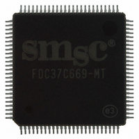
FDC37C669-MT SMSC, FDC37C669-MT Datasheet - Page 79

FDC37C669-MT
Manufacturer Part Number
FDC37C669-MT
Description
IC CTRLR SUPER I/O FLPPY 100TQFP
Manufacturer
SMSC
Datasheet
1.FDC37C669-MT.pdf
(162 pages)
Specifications of FDC37C669-MT
Controller Type
I/O Controller
Interface
ISA Host
Voltage - Supply
4.5 V ~ 5.5 V
Current - Supply
25mA
Operating Temperature
0°C ~ 70°C
Mounting Type
Surface Mount
Package / Case
100-TQFP, 100-VQFP
Lead Free Status / RoHS Status
Lead free / RoHS Compliant
Other names
638-1008
Available stocks
Company
Part Number
Manufacturer
Quantity
Price
Company:
Part Number:
FDC37C669-MT
Manufacturer:
Microchip Technology
Quantity:
10 000
- Current page: 79 of 162
- Download datasheet (619Kb)
Bit 0
Delta Clear To Send (DCTS). Bit 0 indicates that the
nCTS input to the chip has changed state since the
last time the MSR was read.
Bit 1
Delta Data Set Ready (DDSR). Bit 1 indicates that the
nDSR input has changed state since the last time the
MSR was read.
Bit 2
Trailing Edge of Ring Indicator (TERI). Bit 2 indicates
that the nRI input has changed from logic "0" to logic "1".
Bit 3
Delta Data Carrier Detect (DDCD). Bit 3 indicates that
the nDCD input to the chip has changed state.
NOTE: Whenever bit 0, 1, 2, or 3 is set to a logic "1", a
MODEM Status Interrupt is generated.
Bit 4
This bit is the complement of the Clear To Send (nCTS)
input. If bit 4 of the MCR is set to logic "1", this bit is
equivalent to nRTS in the MCR.
Bit 5
This bit is the complement of the Data Set Ready (nDSR)
input. If bit 4 of the MCR is set to logic "1", this bit is
equivalent to DTR in the MCR.
Bit 6
This bit is the complement of the Ring Indicator (nRI)
input. If bit 4 of the MCR is set to logic "1", this bit is
equivalent to OUT1 in the MCR.
Bit 7
This bit is the complement of the Data Carrier Detect
(nDCD) input. If bit 4 of the MCR is set
79
to logic "1", this bit is equivalent to OUT2 in the MCR.
SCRATCHPAD REGISTER (SCR)
Address Offset =7H, DLAB =X, READ/WRITE
This 8 bit read/write register has no effect on the
operation of the Serial Port.
scratchpad register to be used by the programmer to hold
data temporarily.
PROGRAMMABLE BAUD RATE GENERATOR (AND
DIVISOR LATCHES DLH, DLL)
The Serial Port contains a programmable Baud Rate
Generator that is capable of taking any clock input (DC to
3 MHz) and dividing it by any divisor from 1 to 65535.
This output frequency of the Baud Rate Generator is 16x
the Baud rate. Two 8 bit latches store the divisor in 16 bit
binary format. These Divisor Latches must be loaded
during initialization in order to insure desired operation of
the Baud Rate Generator. Upon loading either of the
Divisor Latches, a 16 bit Baud counter is immediately
loaded. This prevents long counts on initial load. If a 0 is
loaded into the BRG registers the output divides the clock
by the number 3. If a 1 is loaded the output is the inverse
of the input oscillator. If a two is loaded the output is a
divide by 2 signal with a 50% duty cycle. If a 3 or greater
is loaded the output is low for 2 bits and high for the
remainder of the count. The input clock to the BRG is the
24 MHz crystal divided by 13, giving a 1.8462 MHz clock.
Table 33 shows the baud rates possible with a 1.8462
MHz crystal.
Effect Of The Reset on Register File
The Reset Function Table (Table 34) details the effect of
the Reset input on each of the registers of the Serial Port.
It is intended as a
Related parts for FDC37C669-MT
Image
Part Number
Description
Manufacturer
Datasheet
Request
R

Part Number:
Description:
FAST ETHERNET PHYSICAL LAYER DEVICE
Manufacturer:
SMSC Corporation
Datasheet:

Part Number:
Description:
357-036-542-201 CARDEDGE 36POS DL .156 BLK LOPRO
Manufacturer:
SMSC Corporation
Datasheet:

Part Number:
Description:
357-036-542-201 CARDEDGE 36POS DL .156 BLK LOPRO
Manufacturer:
SMSC Corporation
Datasheet:

Part Number:
Description:
357-036-542-201 CARDEDGE 36POS DL .156 BLK LOPRO
Manufacturer:
SMSC Corporation
Datasheet:

Part Number:
Description:
4-PORT USB2.0 HUB CONTROLLER
Manufacturer:
SMSC Corporation
Datasheet:

Part Number:
Description:
Manufacturer:
SMSC Corporation
Datasheet:

Part Number:
Description:
Manufacturer:
SMSC Corporation
Datasheet:

Part Number:
Description:
FDC37C672ENHANCED SUPER I/O CONTROLLER WITH FAST IR
Manufacturer:
SMSC Corporation
Datasheet:

Part Number:
Description:
COM90C66LJPARCNET Controller/Transceiver with AT Interface and On-Chip RAM
Manufacturer:
SMSC Corporation
Datasheet:

Part Number:
Description:
Manufacturer:
SMSC Corporation
Datasheet:

Part Number:
Description:
Manufacturer:
SMSC Corporation
Datasheet:

Part Number:
Description:
Manufacturer:
SMSC Corporation
Datasheet:

Part Number:
Description:
Manufacturer:
SMSC Corporation
Datasheet:


